DP83910AN National Semiconductor, DP83910AN Datasheet - Page 6
DP83910AN
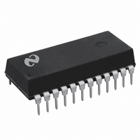
Manufacturer Part Number
DP83910AN
Description
IC SERIAL NETWRK INT CMOS 24-DIP
Manufacturer
National Semiconductor
Datasheet
1.DP83910AVNOPB.pdf
(12 pages)
Specifications of DP83910AN
Applications
Ethernet Network
Interface
Serial
Voltage - Supply
4.75 V ~ 5.25 V
Package / Case
24-DIP (0.300", 7.62mm)
Mounting Type
Through Hole
Lead Free Status / RoHS Status
Contains lead / RoHS non-compliant
Other names
*DP83910AN
Available stocks
Company
Part Number
Manufacturer
Quantity
Price

Part Number:
DP83910AN
Manufacturer:
NS/国半
Quantity:
20 000


Symbol
Controller Interface Pins (COL RXD CRS RXC SEL LBK TXD TXC and TXE)
V
V
I
V
V
I
I
Differential Pins (TX
V
V
V
V
V
Oscillator Pins (X1 and X2)
V
V
I
7 0 Absolute Maximum Ratings
If Military Aerospace specified devices are required
please contact the National Semiconductor Sales
Office Distributors for availability and specifications
Supply Voltage (V
DC Input Voltage (V
DC Output Voltage (V
Differential Input Voltage
Differential Output Voltage
Power Dissipation
Storage Temperature
8 0 DC Specifications
Note 1 This measurement was made while the DP83910A was undergoing transmission reception and collision detection Also this value was not measured
instantaneously but averaged over a span of several milliseconds (V
Note 2 This measurement was made while the DP83910A was sitting idle with TXE low Also this value was not measured instantaneously but averaged over a
span of several milliseconds (V
Note 3 This parameter is guaranteed by design and is not tested
IN
CCO
CCS
OSC
IH
IL
OH
OL
OD
OB
U
DS
CM
IH
IL
Input High Voltage
Input Low Voltage
Input Leakage
Output High Voltage
Output Low Voltage
Operating V
Current (Note 1)
Stand By V
Current (Note 2)
Diff Output Voltage (TX
Diff Output Voltage
Imbalance (TX
Undershoot Voltage (TX
Diff Squelch Threshold
(RX
Diff Input Common Mode
Voltage (RX
(Note 3)
X1 Input High Voltage
X1 Input Low Voltage
X1 Input Current
g
CC
and CD
IN
)
Parameter
g
OUT
)
CC
RX
CC
g
IN
)
g
Supply
g
g
and CD
e
Supply
)
)
2 4V or 0 4V and I
and CD
g
T
g
g
)
A
b
b
g
)
)
e
0 5V to V
0 5V to V
)
b
0 C to 70 C V
65 C to
o
b
V
(TTL) I
(CMOS) I
(TTL) I
(CMOS) I
10 Mbit sec
10 Mbit sec
78
270
78
270
78
270
X1 is connected to an oscillator
and X2 is grounded
X1 is connected to an oscillator
and X2 is grounded
X1
X2
b
e
IN
0 5V to
5 5 to
0 mA)
e
e
e
CC
CC
Termination and
Termination and
Termination and
from each to GND (Figure 4)
from each to GND (Figure 4)
from each to GND (Figure 4)
V
GND
0 to 16V
500 mW
a
OH
OL
V
CC
a
a
CC
a
150 C
OH
OL
a
e
0 5V
0 5V
e
IN
16V
or GND
Conditions
or GND
CC
7V
e
e
2 0 mA
2 0 mA
e
2 4V or 0 4V and I
e
20 A
20 A
5V
6
g
which the safety of the device cannot be guaranteed They
are not meant to imply that the device should be operated at
these limits
Lead Temperature (Soldering 10 sec )
ESD (R
Note Absolute maximum ratings are those values beyond
eter has been characterized but not tested
Note All specifications in this datasheet are valid only if the mandatory
isolation is employed and all differential signals are taken to exist at the AUI
side of the pulse transformer
Note An asterisk following a parameter’s symbol indicates that the param-
5%
o
ZAP
e
0 mA)
e
1 5 k
V
CC
g
b
b
Min
b
2 0
3 5
2 0
550
175
b
0
1 0
C
2
ZAP
0 1
e
120 pF)
Typ
100
40
g
b
(Pin 4
Max
a
0 8
1 0
0 4
0 1
1200
5 5
0 8
70
65
300
2
e
1 5 kV)
t
260 C
Units
2 kV
mA
mA
mV
mV
mV
mV
mA
V
V
V
V
V
V
V
V
V
A
Related parts for DP83910AN
Image
Part Number
Description
Manufacturer
Datasheet
Request
R

Part Number:
Description:
National Semiconductor [8-Bit D/A Converter]
Manufacturer:
National Semiconductor
Datasheet:
Part Number:
Description:
National Semiconductor [Media Coprocessor]
Manufacturer:
National Semiconductor
Datasheet:
Part Number:
Description:
Digitally Controlled Tone and Volume Circuit with Stereo Audio Power Amplifier, Microphone Preamp Stage and National 3D Sound
Manufacturer:
National Semiconductor
Datasheet:
Part Number:
Description:
Digitally Controlled Tone and Volume Circuit with Stereo Audio Power Amplifier, Microphone Preamp Stage and National 3D Sound
Manufacturer:
National Semiconductor
Datasheet:
Part Number:
Description:
AC97 Rev 2 Codec with Sample Rate Conversion and National 3D Sound
Manufacturer:
National Semiconductor
Part Number:
Description:
Manufacturer:
National Semiconductor
Datasheet:
Part Number:
Description:
Manufacturer:
National Semiconductor
Datasheet:
Part Number:
Description:
General Purpose, Low Voltage, Low Power, Rail-to-Rail Output Operational Amplifiers
Manufacturer:
National Semiconductor
Datasheet:
Part Number:
Description:
8-bit 20 MSPS flash A/D converter.
Manufacturer:
National Semiconductor
Datasheet:
Part Number:
Description:
Low Noise Quad Operational Amplifier
Manufacturer:
National Semiconductor
Datasheet:
Part Number:
Description:
Quad Differential Line Receivers
Manufacturer:
National Semiconductor
Datasheet:
Part Number:
Description:
Quad High Speed Trapezoidal? Bus Transceiver
Manufacturer:
National Semiconductor
Datasheet:
Part Number:
Description:
Dual Line Receiver
Manufacturer:
National Semiconductor
Datasheet:
Part Number:
Description:
TTL to 10k ECL Level Translator with Latch
Manufacturer:
National Semiconductor
Datasheet: