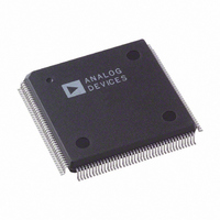
AD9887AKS-140 Analog Devices Inc, AD9887AKS-140 Datasheet - Page 39

AD9887AKS-140
Manufacturer Part Number
AD9887AKS-140
Description
IC INTRFACE ANALOG/DVI 160-MQFP
Manufacturer
Analog Devices Inc
Datasheet
1.AD9887AKSZ-100.pdf
(40 pages)
Specifications of AD9887AKS-140
Rohs Status
RoHS non-compliant
Applications
Graphic Cards, VGA Interfaces
Interface
Analog and Digital
Voltage - Supply
3.15 V ~ 3.45 V
Package / Case
160-MQFP, 160-PQFP
Mounting Type
Surface Mount
Available stocks
Company
Part Number
Manufacturer
Quantity
Price
Company:
Part Number:
AD9887AKS-140
Manufacturer:
AD
Quantity:
275
Company:
Part Number:
AD9887AKS-140
Manufacturer:
TOS
Quantity:
160
Company:
Part Number:
AD9887AKS-140
Manufacturer:
AD
Quantity:
586
Part Number:
AD9887AKS-140
Manufacturer:
ADI/亚德诺
Quantity:
20 000
It is particularly important to maintain low noise and good
stability of PV
PV
phase and frequency. This can be avoided by careful attention
to regulation, filtering, and bypassing. It is highly desirable to
provide separate regulated supplies for each of the analog cir-
cuitry groups (V
Some graphic controllers use substantially different levels of
power when active (during active picture time) and when idle
(during horizontal and vertical sync periods). This can result in
a measurable change in the voltage supplied to the analog
supply regulator, which can in turn produce changes in the
regulated analog supply voltage. This can be mitigated by regu-
lating the analog supply, or at least PV
power source (for example, from a 12 V supply).
It is also recommended to use a single ground plane for the
entire board. Experience has repeatedly shown that the noise
performance is the same or better with a single ground plane.
Using multiple ground planes can be detrimental because each
separate ground plane is smaller, and long ground loops can result.
In some cases, using separate ground planes is unavoidable. For
those cases, it is recommended to at least place a single ground
plane under the AD9887. The location of the split should be at
the receiver of the digital outputs. For this case it is even more
important to place components wisely because the current loops
will be much longer (current takes the path of least resistance).
An example of a current loop:
D
can result in similarly abrupt changes in sampling clock
D
(the clock generator supply). Abrupt changes in
D
and PVD).
D
, from a different, cleaner
PLL
Place the PLL loop filter components as close to the FILT pin
as possible.
Do not place any digital or other high-frequency traces near
these components.
Use the values suggested in the data sheet with 10% tolerances
or less.
Outputs (Both Data and Clocks)
Try to minimize the trace length that the digital outputs have to
drive. Longer traces have higher capacitance, which require
more current that causes more internal digital noise.
Shorter traces reduce the possibility of reflections.
Adding a series resistor of value 50 Ω–200 Ω can suppress reflec-
tions, reduce EMI, and reduce the current spikes inside of the
AD9887. If series resistors are used, place them as close to the
AD9887 pins as possible (try not to add vias or extra length to
the output trace in order to get the resistors closer).
If possible, limit the capacitance that each of the digital outputs
drives to less than 10 pF. This can easily be accomplished by
keeping traces short and by connecting the outputs to only one
device. Loading the outputs with excessive capacitance will
increase the current transients inside of the AD9887 creating
more digital noise on its power supplies.
Digital Inputs
The digital inputs on the AD9887 were designed to work with
3.3 V signals.
Any noise that gets onto the Hsync input trace will add jitter to
the system. Therefore, minimize the trace length and do not run
any digital or other high-frequency traces near it.
Voltage Reference
Bypass with a 0.1 µF capacitor. Place as close to the AD9887
pin as possible. Make the ground connection as short as possible.
REFOUT is easily connected to REFIN with a short trace. Avoid
making this trace any longer than it needs to be.
When using an external reference, the REFOUT output, while
unused, still needs to be bypassed with a 0.1 µF capacitor in
order to avoid ringing.
AD9887


