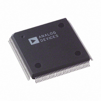
AD9887AKS-140 Analog Devices Inc, AD9887AKS-140 Datasheet - Page 11

AD9887AKS-140
Manufacturer Part Number
AD9887AKS-140
Description
IC INTRFACE ANALOG/DVI 160-MQFP
Manufacturer
Analog Devices Inc
Datasheet
1.AD9887AKSZ-100.pdf
(40 pages)
Specifications of AD9887AKS-140
Rohs Status
RoHS non-compliant
Applications
Graphic Cards, VGA Interfaces
Interface
Analog and Digital
Voltage - Supply
3.15 V ~ 3.45 V
Package / Case
160-MQFP, 160-PQFP
Mounting Type
Surface Mount
Available stocks
Company
Part Number
Manufacturer
Quantity
Price
Company:
Part Number:
AD9887AKS-140
Manufacturer:
AD
Quantity:
275
Company:
Part Number:
AD9887AKS-140
Manufacturer:
TOS
Quantity:
160
Company:
Part Number:
AD9887AKS-140
Manufacturer:
AD
Quantity:
586
Part Number:
AD9887AKS-140
Manufacturer:
ADI/亚德诺
Quantity:
20 000
HSOUT
SOGOUT
Analog Interface
REFOUT
REFIN
FILT
Either or both signals may be used, depend-
ing on the timing mode and interface design
employed.
Horizontal Sync Output
A reconstructed and phase-aligned version of
the Hsync input. Both the polarity and dura-
tion of this output can be programmed via
serial bus registers.
By maintaining alignment with DATACK,
DATACK, and Data, data timing with
respect to horizontal sync can always be
determined.
Sync-On-Green Slicer Output
This pin can be programmed to output
either the output from the Sync-On-Green
slicer comparator or an unprocessed but
delayed version of the HSYNC input. See
the Sync Block Diagram to view how this
pin is connected.
(Note: The output from this pin is the sliced
SOG, without additional processing from the
AD9887.)
Internal Reference Output
Output from the internal 1.25 V bandgap refer-
ence. This output is intended to drive relatively
light loads. It can drive the AD9887 Reference
Input directly, but should be externally buff-
ered if it is used to drive other loads as well.
The absolute accuracy of this output is ± 4%,
and the temperature coefficient is ± 50 ppm,
which is adequate for most AD9887 appli-
cations. If higher accuracy is required, an
external reference may be employed instead.
If an external reference is used, connect this
pin to ground through a 0.1 µF capacitor.
Reference Input
The reference input accepts the master refer-
ence voltage for all AD9887 internal circuitry
(1.25 V ± 10%). It may be driven directly by
the REFOUT pin. Its high impedance pre-
sents a very light load to the reference source.
This pin should always be bypassed to Ground
with a 0.1 µF capacitor.
External Filter Connection
For proper operation, the pixel clock genera-
tor PLL requires an external filter. Connect
the filter shown Figure 7 to this pin. For
optimal performance, minimize noise and
parasitics on this node.
Power Supply
V
V
PV
GND
THEORY OF OPERATION (INTERFACE DETECTION)
Active Interface Detection and Selection
The AD9887 includes circuitry to detect whether or not an
interface is active.
For detecting the analog interface, the circuitry monitors the
presence of HSYNC, VSYNC, and Sync-on-Green. The result of
the detection circuitry can be read from the 2-wire serial inter-
face bus at address 11H Bits 7, 6, and 5 respectively. If one of
these sync signals disappears, the maximum time it takes for the
circuitry to detect it is 100 ms.
There are two stages for detecting the digital interface. The first
stage searches for the presence of the digital interface clock.
The circuitry for detecting the digital interface clock is active
even when the digital interface is powered down. The result of
this detection stage can be read from the 2-wire serial interface
bus at address 11H Bit 4. If the clock disappears, the maximum
time it takes for the circuitry to detect it is 100 ms. The second
stage attempts to detect DE on the digital interface. Detection is
accomplished when 32 DEs have been counted. DE can only be
detected when the digital interface is powered up, so it is not
always active. The DE detection circuitry is one of the logic
inputs used to set the SyncDT output pin (Pin 136). The logic
for the SyncDT pin is [DE detect] OR [HSYNC detect].
There is an override for the automatic interface selection. It is
the AIO bit (Active Interface Override). When the AIO bit is set
to Logic 0, the automatic circuitry will be used. When the AIO
bit is set to Logic 1, the AIS bit will be used to determine the
active interface rather than the automatic circuitry.
D
DD
D
Main Power Supply
These pins supply power to the main elements
of the circuit. It should be filtered to be as
quiet as possible.
Digital Output Power Supply
These supply pins are identified separately
from the V
to minimize output noise transferred into the
sensitive analog circuitry.
If the AD9887 is interfacing with lower-
voltage logic, V
lower supply voltage (as low as 2.2 V) for
compatibility.
Clock Generator Power Supply
The most sensitive portion of the AD9887 is
the clock generation circuitry. These pins
provide power to the clock PLL and help the
user design for optimal performance. The
designer should provide noise-free power to
these pins.
Ground
The ground return for all circuitry on chip.
It is recommended that the application circuit
board have a single, solid ground plane.
D
pins so special care can be taken
DD
may be connected to a
AD9887


