MAX14502AETL+ Maxim Integrated Products, MAX14502AETL+ Datasheet - Page 9
MAX14502AETL+
Manufacturer Part Number
MAX14502AETL+
Description
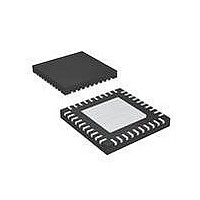
IC CARD READER USB-SD 40-TQFN
Manufacturer
Maxim Integrated Products
Type
Smart Card Interface ICr
Datasheet
1.MAX14502AETL.pdf
(41 pages)
Specifications of MAX14502AETL+
Applications
USB
Interface
I²C
Voltage - Supply
1.8 V ~ 3.3 V
Package / Case
40-TQFN Exposed Pad
Mounting Type
Surface Mount
Maximum Operating Temperature
+ 85 C
Minimum Operating Temperature
- 40 C
Mounting Style
SMD/SMT
Lead Free Status / RoHS Status
Lead free / RoHS Compliant


INPUTS/OUTPUTS
USB INTERFACE
SD CARD INTERFACE
TQFN
25
27
22
21
20
19
28
13
12
11
1
2
3
4
6
7
8
9
PIN
WLP
C4
C6
G7
G8
C8
C7
A2
B4
A3
B6
A7
B7
E6
F5
F7
F8
E5
B8
_______________________________________________________________________________________
BERR/INT
CDAT1_0
CDAT1_1
CDAT1_2
I2C_SEL
KVBUS
NAME
MODE
BUSY
FREF
RREF
ADD
CD+
HD+
SCL
SDA
RST
CD-
HD-
I
I2C_SEL low to disable I
I
the I
I
I
I
slave addresses: (GND = 1110 000Xb and V
Card Reader Error/Interrupt Output. BERR/INT becomes BERR for simple control and
INT for I
during simple control and asserts for enabled interrupts during I
Busy Output. BUSY asserts low to indicate device is in Card Reader mode.
Card Reader/Pass Thru Mode Select Input. MODE is only active during simple
control. Drive MODE low to enable Pass Thru mode and drive MODE high to enable
Card Reader mode. For I
Reset Input. Drive RST low to reset the internal registers to default values and put all
outputs in high impedance. Connect RST to V
Frequency Input. FREF is the clock input (12MHz/13MHz/19.2MHz/26MHz) for the
internal logic and USB PHY. FREF can accept a square-wave or sine-wave clock. An
internal clock squaring circuit can be enabled or disabled through I
control, the internal clock squarer is enabled by default.
Reference Resistor. Connect a Bias Resistor 6.19kΩ ±1% from RREF to GND.
USB Analog Switch/Hi-Speed USB Transceiver. CD+ connects to D+ on the USB
connector.
USB Analog Switch/Hi-Speed USB Transceiver. CD- connects to D- on the USB
connector.
USB Analog Switch. HD+ connects to D+ on the host side.
USB Analog Switch. HD- connects to D- on the host side.
USB Bus Power-Supply Detection Input. Connect a resistor-divider between USB
VBUS, KVBUS, and GND.
SD Card 1 Data Bus Analog Switch/Card Reader Interface. CDAT1_0 connects to
DAT0 on the SD card.
SD Data Card 1 Bus Analog Switch/Card Reader Interface. CDAT1_1 connects to
DAT1 on the SD card.
SD Data Card 1 Bus Analog Switch/Card Reader Interface. CDAT1_2 connects to
DAT2 on the SD card.
2
2
2
2
2
C Select Input. I2C_SEL must be connected to V
C Serial-Clock Input. SCL is +3.6V tolerant and the high threshold is set by V
C Serial-Data I/O. SDA is +3.6V tolerant and the high threshold is set by V
C interface is not used, connect SDA to GND.
C Address Selection Input. Connect ADD to V
2
C interface is not used, connect SCL to GND.
2
C control. BERR/INT goes low to indicate an error in Card Reader mode
Hi-Speed USB-to-SD Card
2
2
C control and drive I2C_SEL high to enable I
C control, MODE must be connected to GND.
Readers with Bypass
FUNCTION
IO
IO
= 1110 001Xb).
IO
for normal operation.
or GND to select between two I
IO
or GND at power-up. Drive
Pin Description
2
C control.
2
C. In simple
2
C control.
IO
. If the
IO
. If
2
C
9
Related parts for MAX14502AETL+
Image
Part Number
Description
Manufacturer
Datasheet
Request
R

Part Number:
Description:
MAX CLIP
Manufacturer:
Aavid Thermalloy
Datasheet:

Part Number:
Description:
MAX7528KCWPMaxim Integrated Products [CMOS Dual 8-Bit Buffered Multiplying DACs]
Manufacturer:
Maxim Integrated Products
Datasheet:
Part Number:
Description:
Single +5V, fully integrated, 1.25Gbps laser diode driver.
Manufacturer:
Maxim Integrated Products
Datasheet:
Part Number:
Description:
Single +5V, fully integrated, 155Mbps laser diode driver.
Manufacturer:
Maxim Integrated Products
Datasheet:
Part Number:
Description:
VRD11/VRD10, K8 Rev F 2/3/4-Phase PWM Controllers with Integrated Dual MOSFET Drivers
Manufacturer:
Maxim Integrated Products
Datasheet:
Part Number:
Description:
Highly Integrated Level 2 SMBus Battery Chargers
Manufacturer:
Maxim Integrated Products
Datasheet:
Part Number:
Description:
Current Monitor and Accumulator with Integrated Sense Resistor; ; Temperature Range: -40°C to +85°C
Manufacturer:
Maxim Integrated Products
Part Number:
Description:
TSSOP 14/A�/RS-485 Transceivers with Integrated 100O/120O Termination Resis
Manufacturer:
Maxim Integrated Products
Part Number:
Description:
TSSOP 14/A�/RS-485 Transceivers with Integrated 100O/120O Termination Resis
Manufacturer:
Maxim Integrated Products
Part Number:
Description:
QFN 16/A�/AC-DC and DC-DC Peak-Current-Mode Converters with Integrated Step
Manufacturer:
Maxim Integrated Products
Part Number:
Description:
TDFN/A/65V, 1A, 600KHZ, SYNCHRONOUS STEP-DOWN REGULATOR WITH INTEGRATED SWI
Manufacturer:
Maxim Integrated Products
Part Number:
Description:
Integrated Temperature Controller f
Manufacturer:
Maxim Integrated Products
Part Number:
Description:
SOT23-6/I�/45MHz to 650MHz, Integrated IF VCOs with Differential Output
Manufacturer:
Maxim Integrated Products
Part Number:
Description:
SOT23-6/I�/45MHz to 650MHz, Integrated IF VCOs with Differential Output
Manufacturer:
Maxim Integrated Products
Part Number:
Description:
EVALUATION KIT/2.4GHZ TO 2.5GHZ 802.11G/B RF TRANSCEIVER WITH INTEGRATED PA
Manufacturer:
Maxim Integrated Products