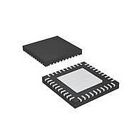
MAX14502AETL+ Maxim Integrated Products, MAX14502AETL+ Datasheet - Page 29

MAX14502AETL+
Manufacturer Part Number
MAX14502AETL+
Description
IC CARD READER USB-SD 40-TQFN
Manufacturer
Maxim Integrated Products
Type
Smart Card Interface ICr
Datasheet
1.MAX14502AETL.pdf
(41 pages)
Specifications of MAX14502AETL+
Applications
USB
Interface
I²C
Voltage - Supply
1.8 V ~ 3.3 V
Package / Case
40-TQFN Exposed Pad
Mounting Type
Surface Mount
Maximum Operating Temperature
+ 85 C
Minimum Operating Temperature
- 40 C
Mounting Style
SMD/SMT
Lead Free Status / RoHS Status
Lead free / RoHS Compliant
A write to the MAX14500–MAX14503 comprises the
transmission of the slave address with the R/W bit set to
zero, followed by at least 1 byte of information. The first
byte of information is the register address or command
byte. The register address determines which register of
the MAX14500–MAX14503 is to be written by the next
byte if received. If a STOP condition is detected after
the register address is received, then the MAX14500–
MAX14503 take no further action beyond storing the
register address (Figure 17).
Any bytes received after the register address are data
bytes. The first data byte goes into the register selected
by the register address and subsequent data bytes go
into subsequent registers (Figure 18). If multiple data
bytes are transmitted before a STOP condition, these
bytes are stored in subsequent registers because the
register address autoincrements.
The MAX14500–MAX14503 are read using the internal-
ly stored register address as an address pointer, the
same way the stored register address is used as an
address pointer for a write. The pointer autoincrements
Figure 17. Format for I
Figure 18. Format for Writing to Multiple Registers. In this example, registers 0x01 and 0x02 are written in sequence.
S
D7
1
D7
S
______________________________________________________________________________________
2
C Write. In this example the register 0x01 is written.
D6
D6
1
1
REGISTER 0x01 WRITE DATA
D5
REGISTER 0x01 WRITE DATA
D5
1
1
ADDRESS = 0xE0
D4
0
D4
1
ADDRESS = 0xE0
D3
0
D3
Format for Reading
0
Format for Writing
D2
D2
0
0
D1
0
D1
0
0 = WRITE
D0
0
D0
0
0 = WRITE
A/A
A
A
0
Hi-Speed USB-to-SD Card
A
P
D7
0
after each data byte is read using the same rules used
for a write. Thus, a read is initiated by first configuring
the register address by performing a write (Figure 19).
The master can now read consecutive bytes from the
MAX14500–MAX14503, with the first data byte being
read from the register addressed pointed by the previ-
ously written register address (Figure 20). Once the
master sends a NACK, the MAX14500–MAX14503 stop
sending valid data.
The MAX14500–MAX14503 support one or two SD
cards or SD interface NAND flash memory.
There are three operational configurations:
• 40-pin TQFN version, containing one host port and
• 56-bump WLP version, containing two SD host ports
D6
0
0
one SD card (Figures 1, 2)
and two SD cards. There are two SD hosts and two
SD memory cards. Use this mode if the host has two
SD ports (Figure 3).
REGISTER 0x02 WRITE DATA
S = START BIT
P = STOP BIT
A = ACK
A = NACK
D_ = DATA BIT
Readers with Bypass
REGISTER ADDRESS = 0x01
D5
0
0
D4
0
REGISTER ADDRESS = 0x01
0
D3
0
0
Applications Information
D2
0
0
D1
0
0
D0
1
0
A/A
A
1
SD Ports Configuration
P
A
SD Ports
29


