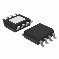
AOZ1037PI Alpha & Omega Semiconductor Inc, AOZ1037PI Datasheet - Page 10

AOZ1037PI
Manufacturer Part Number
AOZ1037PI
Description
IC BUCK SYNC ADJ 5A SO8
Manufacturer
Alpha & Omega Semiconductor Inc
Series
EZBuck™r
Type
Step-Down (Buck), PWM - Current Moder
Datasheet
1.AOZ1037PI.pdf
(14 pages)
Specifications of AOZ1037PI
Featured Product
The AOZ103x Family Synchronous Buck Regulator
Internal Switch(s)
Yes
Synchronous Rectifier
Yes
Number Of Outputs
1
Voltage - Output
0.8 V ~ 18 V
Current - Output
5A
Frequency - Switching
500kHz
Voltage - Input
4.5 V ~ 18 V
Operating Temperature
-40°C ~ 85°C
Mounting Type
Surface Mount
Package / Case
8-SOIC (0.154", 3.90mm Width) Exposed Pad
Lead Free Status / Rohs Status
Lead free / RoHS Compliant
Other names
785-1256-2
Available stocks
Company
Part Number
Manufacturer
Quantity
Price
Company:
Part Number:
AOZ1037PI
Manufacturer:
AOS
Quantity:
884
Part Number:
AOZ1037PI
Manufacturer:
AOS/万代
Quantity:
20 000
For lower output ripple voltage across the entire
operating temperature range, X5R or X7R dielectric type
of ceramic, or other low ESR tantalum are recommended
to be used as output capacitors.
In a buck converter, output capacitor current is
continuous. The RMS current of output capacitor is
decided by the peak to peak inductor ripple current. It
can be calculated by:
Usually, the ripple current rating of the output capacitor is
a smaller issue because of the low current stress. When
the buck inductor is selected to be very small and
inductor ripple current is high, output capacitor could be
overstressed.
External Schottky Diode for High Input Operation
When V
diode is required between LX and PGND for proper
operation.
Loop Compensation
The AOZ1037 employs peak current mode control for
easy use and fast transient response. Peak current mode
control eliminates the double pole effect of the output
L&C filter. It greatly simplifies the compensation loop
design.
With peak current mode control, the buck power stage
can be simplified to be a one-pole and one-zero system
in frequency domain. The pole is dominant pole can be
calculated by:
The zero is a ESR zero due to output capacitor and its
ESR. It is can be calculated by:
where;
C
R
ESR
The compensation design is actually to shape the
converter control loop transfer function to get desired
gain and phase. Several different types of compensation
I
f
CO_RMS
O
L
Z1
f
Rev. 1.1 September 2010
P1
is load resistor value, and
is the output filter capacitor,
CO
=
=
is the equivalent series resistance of output capacitor.
IN
------------------------------------------------
2π C
---------------------------------- -
2π C
is higher than 16V, an external 1A schottky
=
×
×
----------
ΔI
O
12
1
O
L
1
×
×
ESR
R
L
CO
www.aosmd.com
network can be used for the AOZ1037. For most cases, a
series capacitor and resistor network connected to the
COMP pin sets the pole-zero and is adequate for a stable
high-bandwidth control loop.
In the AOZ1037, FB pin and COMP pin are the inverting
input and the output of internal error amplifier. A series
R and C compensation network connected to COMP
provides one pole and one zero. The pole is:
where;
G
A/V,
G
C
The zero given by the external compensation network,
capacitor C
To design the compensation circuit, a target crossover
frequency f
crossover frequency is where control loop has unity gain.
The crossover is the also called the converter bandwidth.
Generally a higher bandwidth means faster response to
load transient. However, the bandwidth should not be too
high because of system stability concern. When
designing the compensation loop, converter stability
under all line and load condition must be considered.
Usually, it is recommended to set the bandwidth to be
equal or less than 1/10 of switching frequency. The
AOZ1037 operates at a frequency range from 400kHz to
600kHz. It is recommended to choose a crossover
frequency equal or less than 40kHz.
The strategy for choosing R
over frequency with R
with C
calculate R
f
f
R
f
C
P2
EA
VEA
2
Z2
C
is the compensation capacitor in Figure 1.
=
is the error amplifier transconductance, which is 200 x 10
=
is the error amplifier voltage gain, which is 500 V/V, and
=
=
C
40kHz
. Using selected crossover frequency, f
----------------------------------------- -
2π
--------------------------------- -
2π
f
C
×
C
C
2
×
×
:
for close loop must be selected. The system
and resistor R
--------- -
V
C
V
C
G
1
FB
O
2
2
EA
×
×
×
G
R
----------------------------- -
G
3
VEA
C
2π C
EA
and set the compensator zero
×
×
3
C
G
, is located at:
and C
2
CS
C
is to set the cross
AOZ1037
Page 10 of 14
C
, to
-6


