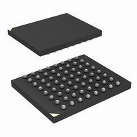
RC28F320J3D75B Numonyx - A DIVISION OF MICRON SEMICONDUCTOR PRODUCTS, INC., RC28F320J3D75B Datasheet - Page 39

RC28F320J3D75B
Manufacturer Part Number
RC28F320J3D75B
Description
IC FLASH 32MBIT 75NS 64EZBGA
Manufacturer
Numonyx - A DIVISION OF MICRON SEMICONDUCTOR PRODUCTS, INC.
Series
-r
Datasheet
1.RC28F128J3D75B.pdf
(66 pages)
Specifications of RC28F320J3D75B
Format - Memory
FLASH
Memory Type
FLASH
Memory Size
32M (4Mx8, 2Mx16)
Speed
75ns
Interface
Parallel
Voltage - Supply
2.7 V ~ 3.6 V
Operating Temperature
-40°C ~ 85°C
Package / Case
64-EZBGA
Lead Free Status / Rohs Status
Contains lead / RoHS non-compliant
Other names
872859
872859TR
872859TR
RC28F320J3D75 S L8QS
RC28F320J3D75B
RC28F320J3D75BTR
872859TR
872859TR
RC28F320J3D75 S L8QS
RC28F320J3D75B
RC28F320J3D75BTR
Available stocks
Company
Part Number
Manufacturer
Quantity
Price
Company:
Part Number:
RC28F320J3D75B
Manufacturer:
Micron Technology Inc
Quantity:
10 000
Numonyx™ Embedded Flash Memory (J3 v D, Monolithic)
9.3.1
Note:
9.3.2
Note:
Note:
December 2007
316577-06
Single-Word/Byte Programming
Array programming is performed by first issuing the Single-Word/Byte Program
command. This is followed by writing the desired data at the desired array address. The
read mode of the device is automatically changed to Read Status Register mode, which
remains in effect until another read-mode command is issued.
During programming, STS and the Status Register indicate a busy status (SR.7 = 0).
Upon completion, STS and the Status Register indicate a ready status (SR.7 = 1). The
Status Register should be checked for any errors (SR.4), then cleared.
Issuing the Read Array command to the device while it is actively programming causes
subsequent reads from the device to output invalid data. Valid array data is output only
after the program operation has finished.
Standby power levels are not be realized until the programming operation has finished.
Also, asserting RP# aborts the programming operation, and array contents at the
addressed location are indeterminate. The addressed block should be erased, and the
data re-programmed. If a Single-Word/Byte program is attempted when the
corresponding block lock-bit is set, SR.1 and SR.4 will be set.
Buffered Programming
Buffered programming operations simultaneous program multiple words into the flash
memory array, significantly reducing effective word-write times. User-data is first
written to a write buffer, then programmed into the flash memory array in buffer-size
increments. For additional details, see the flow chart of the buffered-programming
operation.
Optimal performance and power consumption is realized only by aligning the start
address on 32-word boundaries (i.e., A[4:0] = 0b00000b). Crossing a 32-word
boundary during a buffered programming operation can cause programming time to
double.
To perform a buffered programming operation, first issue the Buffered Program setup
command at the desired starting address. The read mode of the device/addressed
partition is automatically changed to Read Status Register mode.
Polling SR.7 determines write-buffer availability (0 = not available, 1 = available). If
the write buffer is not available, re-issue the setup command and check SR.7; repeat
until SR.7 = 1.
Next, issue the word count at the desired starting address. The word count represents
the total number of words to be written into the write buffer, minus one. This value can
range from 00h (one word) to a maximum of 1Fh (32 words). Exceeding the allowable
range causes an abort.
Following the word count, the write buffer is filled with user-data. Subsequent bus-
write cycles provide addresses and data, up to the word count. All user-data addresses
must lie between <starting address> and <starting address + word count>, otherwise
the WSM continues to run as normal but, user may advertently change the content in
unexpected address locations.
User-data is programmed into the flash array at the address issued when filling the
write buffer.
After all user-data is written into the write buffer, issue the confirm command. If a
command other than the confirm command is issued to the device, a command
sequence error occurs and the operation aborts.
Datasheet
39


