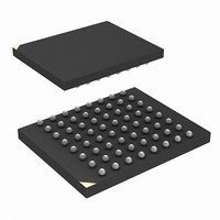
PC28F128J3D75B Numonyx - A DIVISION OF MICRON SEMICONDUCTOR PRODUCTS, INC., PC28F128J3D75B Datasheet - Page 9

PC28F128J3D75B
Manufacturer Part Number
PC28F128J3D75B
Description
IC FLASH 128MBIT 75NS 64EZBGA
Manufacturer
Numonyx - A DIVISION OF MICRON SEMICONDUCTOR PRODUCTS, INC.
Series
-r
Datasheet
1.RC28F128J3D75B.pdf
(66 pages)
Specifications of PC28F128J3D75B
Format - Memory
FLASH
Memory Type
FLASH
Memory Size
128M (16Mx8, 8Mx16)
Speed
75ns
Interface
Parallel
Voltage - Supply
2.7 V ~ 3.6 V
Operating Temperature
-40°C ~ 85°C
Package / Case
64-TBGA
Lead Free Status / Rohs Status
Lead free / RoHS Compliant
Other names
872768
872768TR
872768TR
PC28F128J3D75 872768
PC28F128J3D75B
PC28F128J3D75BTR
872768TR
872768TR
PC28F128J3D75 872768
PC28F128J3D75B
PC28F128J3D75BTR
Available stocks
Company
Part Number
Manufacturer
Quantity
Price
Company:
Part Number:
PC28F128J3D75B
Manufacturer:
Micron Technology Inc
Quantity:
10 000
Numonyx™ Embedded Flash Memory (J3 v D, Monolithic)
December 2007
316577-06
Memory Blocks are selectively and individually lockable in-system. Individual block
locking uses block lock-bits to lock and unlock blocks. Block lock-bits gate block erase
and program operations. Lock-bit configuration operations set and clear lock-bits (using
the Set Block Lock-Bit and Clear Block Lock-Bits commands).
The Status Register indicates when the WSM’s block erase, program, or lock-bit
configuration operation completes.
The STS (status) output gives an additional indicator of WSM activity by providing both
a hardware signal of status (versus software polling) and status masking (interrupt
masking for background block erase, for example). Status indication using STS
minimizes both CPU overhead and system power consumption. When configured in
level mode (default mode), it acts as a RY/BY# signal. When low, STS indicates that the
WSM is performing a block erase, program, or lock-bit configuration. STS-high indicates
that the WSM is ready for a new command, block erase is suspended (and
programming is inactive), program is suspended, or the device is in reset/power-down
mode. Additionally, the configuration command allows the STS signal to be configured
to pulse on completion of programming and/or block erases.
Three CE signals are used to enable and disable the device. A unique CE logic design
(see
reduces decoder logic typically required for multi-chip designs. External logic is not
required when designing a single chip, a dual chip, or a 4-chip miniature card or SIMM
module.
The BYTE# signal allows either x8 or x16 read/writes to the device:
Figure 1, “Memory Block Diagram, 32-, 64-, 128-, and 256-Mbit (monolithic)” on
page 10
When the device is disabled (see
and 256-Mb” on page
enabled. When RP# is at VIL, a further power-down mode is enabled which minimizes
power consumption and provides write protection during reset. A reset time (tPHQV) is
required from RP# going high until data outputs are valid. Likewise, the device has a
wake time (tPHWL) from RP#-high until writes to the CUI are recognized. With RP# at
VIL, the WSM is reset and the Status Register is cleared.
• BYTE#-low enables 8-bit mode; address A0 selects between the low byte and high
• BYTE#-high enables16-bit operation; address A1 becomes the lowest order
byte.
address and address A0 is not used (don’t care).
Table 16, “Chip Enable Truth Table for 32-, 64-, 128- and 256-Mb” on page
shows a device block diagram.
31), with CEx at VIH and RP# at VIH, the standby mode is
Table 16, “Chip Enable Truth Table for 32-, 64-, 128-
Datasheet
31)
9


