DP83816AVNG/NOPB National Semiconductor, DP83816AVNG/NOPB Datasheet - Page 5
DP83816AVNG/NOPB
Manufacturer Part Number
DP83816AVNG/NOPB
Description
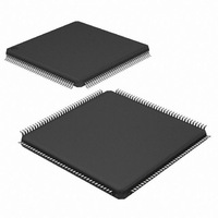
IC MEDIA ACCESS CTRLR 144-LQFP
Manufacturer
National Semiconductor
Datasheet
1.DP83816AVNGNOPB.pdf
(106 pages)
Specifications of DP83816AVNG/NOPB
Applications
*
Interface
*
Voltage - Supply
*
Package / Case
144-LQFP
Mounting Type
Surface Mount
For Use With
DP83816-MAAP - BOARD EVALUATION DP83816
Lead Free Status / RoHS Status
Lead free / RoHS Compliant
Other names
*DP83816AVNG
*DP83816AVNG/NOPB
DP83816AVNG
*DP83816AVNG/NOPB
DP83816AVNG
Available stocks
Company
Part Number
Manufacturer
Quantity
Price
Company:

Part Number:
DP83816AVNG/NOPB
Manufacturer:
NS
Quantity:
5 000
Company:
Part Number:
DP83816AVNG/NOPB
Manufacturer:
Texas Instruments
Quantity:
10 000
Part Number:
DP83816AVNG/NOPB
Manufacturer:
NS/国半
Quantity:
20 000


2.0 Pin Description
PCI Bus Interface
AD[31-0]
CBEN[3-0]
PCICLK
DEVSELN
FRAMEN
GNTN
IDSEL
INTAN
IRDYN
PAR
PERRN
REQN
RSTN
Symbol
66, 67, 68, 70,
71, 72, 73, 74,
78, 79, 81, 82,
83, 86, 87, 88,
101, 102, 104,
105, 106, 108,
109, 110, 112,
113, 115, 116,
118, 119, 120,
LQFP Pin
No(s)
100,
121
111
75,
89,
60
95
91
63
76
61
92
99
97
64
62
Dir
I/O
I/O
I/O
I/O
I/O
I/O
I/O
O
O
I
I
I
I
Address and Data: Multiplexed address and data bus. As a bus master, the
DP83816 will drive address during the first bus phase. During subsequent phases,
the DP83816 will either read or write data expecting the target to increment its
address pointer. As a bus target, the DP83816 will decode each address on the bus
and respond if it is the target being addressed.
Bus Command/Byte Enable: During the address phase these signals define the
“bus command” or the type of bus transaction that will take place. During the data
phase these pins indicate which byte lanes contain valid data. CBEN[0] applies to
byte 0 (bits 7-0) and CBEN[3] applies to byte 3 (bits 31-24) in the Little Endian
Mode. In Big Endian Mode, CBEN[3] applies to byte 0 (bits 31-24) and CBEN[0]
applies to byte 3 (bits 7-0).
Clock: This PCI Bus clock provides timing for all bus phases. The rising edge
defines the start of each phase. The clock frequency ranges from 0 to 33 MHz.
Device Select: As a bus master, the DP83816 samples this signal to insure that the
destination address for the data transfer is recognized by a PCI target. As a target,
the DP83816 asserts this signal low when it recognizes its address after FRAMEN
is asserted.
Frame: As a bus master, this signal is asserted low to indicate the beginning and
duration of a bus transaction. Data transfer takes place when this signal is asserted.
It is de-asserted before the transaction is in its final phase. As a target, the device
monitors this signal before decoding the address to check if the current transaction
is addressed to it.
Grant: This signal is asserted low to indicate to the DP83816 that it has been
granted ownership of the bus by the central arbiter. This input is used when the
DP83816 is acting as a bus master.
Initialization Device Select: This pin is sampled by the DP83816 to identify when
configuration read and write accesses are intended for it.
Interrupt A: This signal is asserted low when an interrupt condition occurs as
defined in the Interrupt Status Register, Interrupt Mask, and Interrupt Enable
registers.
Initiator Ready: As a bus master, this signal will be asserted low when the
DP83816 is ready to complete the current data phase transaction. This signal is
used in conjunction with the TRYDN signal. Data transaction takes place at the
rising edge of PCICLK when both IRDYN and TRDYN are asserted low. As a target,
this signal indicates that the master has put the data on the bus.
Parity: This signal indicates even parity across AD[31-0] and CBEN[3-0] including
the PAR pin. As a master, PAR is asserted during address and write data phases.
As a target, PAR is asserted during read data phases.
Parity Error: The DP83816 as a master or target will assert this signal low to
indicate a parity error on any incoming data (except for special cycles). As a bus
master, it will monitor this signal on all write operations (except for special cycles).
Request: The DP83816 will assert this signal low to request ownership of the bus
from the central arbiter.
Reset: When this signal is asserted all PCI bus outputs of DP83816 will be in TRI-
STATE
®
and the device will be put into a known state.
5
Description
www.national.com
Related parts for DP83816AVNG/NOPB
Image
Part Number
Description
Manufacturer
Datasheet
Request
R

Part Number:
Description:
DP83816 10/100 Mb/s Integrated PCI Ethernet Media Access Controller and Physical Layer (MacPHYTER-II)
Manufacturer:
National Semiconductor
Datasheet:
Part Number:
Description:
BOARD EVALUATION DP83816
Manufacturer:
National Semiconductor
Datasheet:
Part Number:
Description:
National Semiconductor [8-Bit D/A Converter]
Manufacturer:
National Semiconductor
Datasheet:
Part Number:
Description:
National Semiconductor [Media Coprocessor]
Manufacturer:
National Semiconductor
Datasheet:
Part Number:
Description:
Digitally Controlled Tone and Volume Circuit with Stereo Audio Power Amplifier, Microphone Preamp Stage and National 3D Sound
Manufacturer:
National Semiconductor
Datasheet:
Part Number:
Description:
Digitally Controlled Tone and Volume Circuit with Stereo Audio Power Amplifier, Microphone Preamp Stage and National 3D Sound
Manufacturer:
National Semiconductor
Datasheet:
Part Number:
Description:
AC97 Rev 2 Codec with Sample Rate Conversion and National 3D Sound
Manufacturer:
National Semiconductor
Part Number:
Description:
Manufacturer:
National Semiconductor
Datasheet:
Part Number:
Description:
Manufacturer:
National Semiconductor
Datasheet:
Part Number:
Description:
General Purpose, Low Voltage, Low Power, Rail-to-Rail Output Operational Amplifiers
Manufacturer:
National Semiconductor
Datasheet:
Part Number:
Description:
8-bit 20 MSPS flash A/D converter.
Manufacturer:
National Semiconductor
Datasheet:
Part Number:
Description:
Low Noise Quad Operational Amplifier
Manufacturer:
National Semiconductor
Datasheet:
Part Number:
Description:
Quad Differential Line Receivers
Manufacturer:
National Semiconductor
Datasheet:
Part Number:
Description:
Quad High Speed Trapezoidal? Bus Transceiver
Manufacturer:
National Semiconductor
Datasheet: