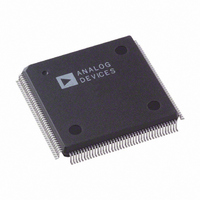
AD9887AKSZ-170 Analog Devices Inc, AD9887AKSZ-170 Datasheet - Page 33

AD9887AKSZ-170
Manufacturer Part Number
AD9887AKSZ-170
Description
IC INTRFACE ANALOG/DVI 160-MQFP
Manufacturer
Analog Devices Inc
Specifications of AD9887AKSZ-170
Applications
Graphic Cards, VGA Interfaces
Interface
Analog and Digital
Voltage - Supply
3.15 V ~ 3.45 V
Package / Case
160-MQFP, 160-PQFP
Mounting Type
Surface Mount
Supply Voltage Range
3.15V To 3.45V, 2.2V To 3.45V
Operating Temperature Range
0°C To +70°C
Digital Ic Case Style
MQFP
No. Of Pins
160
Msl
MSL 3 - 168 Hours
Termination Type
SMD
Rohs Compliant
Yes
Filter Terminals
SMD
Bandwidth
170MHz
Lead Free Status / RoHS Status
Lead free / RoHS Compliant
Available stocks
Company
Part Number
Manufacturer
Quantity
Price
Company:
Part Number:
AD9887AKSZ-170
Manufacturer:
ADI
Quantity:
437
Company:
Part Number:
AD9887AKSZ-170
Manufacturer:
Analog Devices Inc
Quantity:
10 000
Part Number:
AD9887AKSZ-170
Manufacturer:
AD
Quantity:
20 000
Address
0x10
0x11
0x12
Read and
Write, or
Read Only
R/W
RO
R/W
Bits
7:2
7:1
7:0
Default
Value
***1****
****0***
*****0**
******0*
*******0
0*******
*0******
**11****
****0***
*****1**
1*******
*1******
**1*****
***1****
****1***
*****1**
******1*
0*******
*0******
**0*****
***0****
****0***
Register Name
Mode Control 2
Sync Detection
and Active
Interface Control
Active Interface
Rev. B | Page 33 of 52
Description
Bit 4—Clamp Input Signal Polarity (name also same as Bit 6). Valid only
with external CLAMP signal. Logic 0 = active low; Logic 1 = active high.
Bit 3—External Clock Select (EXTCLK). Shuts down the PLL and allows
the use of an external clock to drive the part. Logic 0 = uses internal
PLL; Logic 1 = bypasses the internal PLL.
Bit 2—Red Clamp Select. Logic 0 selects clamp to ground; Logic 1
selects clamp to midscale. (Voltage at Pin 120 and 118)
Bit 1—Green Clamp Select. Logic 0 selects clamp to ground; Logic 1
selects clamp to midscale. (Voltage at Pin 111 and 109)
Bit 0—Blue Clamp Select. Logic 0 selects clamp to ground; Logic 1
selects clamp to midscale. (Voltage at Pin 101 and 99)
Bit 7—CKINV: Data Output Clock Invert. Logic 0 = not inverted;
Logic 1 = inverted (digital interface only).
Bit 6—Pixel Select. Selects either one or two pixels per clock mode.
Logic 0 = one pixel/clock; Logic 1 = two pixels/clock (digital interface
only).
Bit 5, 4—Output Drive. Selects among high, medium, and low output
drive strength. Logic 11 or Logic 10 = high, Logic 01 = medium, and
Logic 00 = low.
Bit 3—PDO: High Impedance Outputs. Logic 0 = normal; Logic 1 =
high impedance.
Bit 2—Sync Detect Polarity. This bit sets the polarity for the S
Logic 1 = active high; Logic 0 = active low.
Bit 7—Analog Interface HSYNC Detect. It is set to Logic 1 if Hsync is
present on the analog interface; otherwise, it is set to Logic 0.
Bit 6—Analog Interface Sync-on-Green Detect. It is set to Logic 1 if
sync is present on the green video input; otherwise, it is set to 0.
Bit 5—Analog Interface VSYNC Detect. It is set to Logic 1 if Vsync is
present on the analog interface; otherwise, it is set to Logic 0.
Bit 4—Digital Interface Clock Detect. It is set to Logic 1 if the clock is
present on the digital interface; otherwise, it is set to Logic 0.
Bit 3—Active Interface (AI). This bit indicates which interface is active.
Logic 0 = analog interface; Logic 1 = digital interface.
Bit 2—Active Hsync (AHS). This bit indicates which analog Hsync is being
used. Logic 0 = HSYNC input pin; Logic 1 = Hsync from sync-on-green.
Bit 1—Active Vsync (AVS). This bit indicates which analog Vsync is being
used. Logic 0 = VSYNC input pin; Logic 1 = Vsync from sync-on-green.
Bit 7—Active Interface Override (AIO). If set to Logic 1, the user can
select the active interface via Bit 6. If set to Logic 0, the active
interface is selected via Bit 3 in Register 0x11.
Bit 6—Active Interface Select (AIS). Logic 0 selects the analog interface
as active. Logic 1 selects the digital interface as active. Note that the
indicated interface is active only if Bit 7 is set to Logic 1 or if both
interfaces are active (Bit 6 or Bit 7 and Bit 4 = Logic 1 in Register 0x11).
Bit 5—Active Hsync Override. If set to Logic 1, the user can select the
Hsync to be used via Bit 4. If set to Logic 0, the active interface is
selected via Bit 2 in Register 0x11.
Bit 4—Active Hsync Select. Logic 0 selects Hsync as the active sync.
Logic 1 selects sync-on-green as the active sync. Note that the indicated
Hsync is used only if Bit 5 is set to Logic 1 or if both syncs are active
(Bit 6 and Bit 7 = Logic 1 in Register 0x11).
Bit 3—Active Vsync Override. If set to Logic 1, the user can select the
Vsync to be used via Bit 2. If set to Logic 0, the active interface is
selected via Bit 1 in Register 0x11.
AD9887A
CDT
pin.


