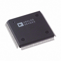
AD9887AKSZ-170 Analog Devices Inc, AD9887AKSZ-170 Datasheet - Page 19

AD9887AKSZ-170
Manufacturer Part Number
AD9887AKSZ-170
Description
IC INTRFACE ANALOG/DVI 160-MQFP
Manufacturer
Analog Devices Inc
Specifications of AD9887AKSZ-170
Applications
Graphic Cards, VGA Interfaces
Interface
Analog and Digital
Voltage - Supply
3.15 V ~ 3.45 V
Package / Case
160-MQFP, 160-PQFP
Mounting Type
Surface Mount
Supply Voltage Range
3.15V To 3.45V, 2.2V To 3.45V
Operating Temperature Range
0°C To +70°C
Digital Ic Case Style
MQFP
No. Of Pins
160
Msl
MSL 3 - 168 Hours
Termination Type
SMD
Rohs Compliant
Yes
Filter Terminals
SMD
Bandwidth
170MHz
Lead Free Status / RoHS Status
Lead free / RoHS Compliant
Available stocks
Company
Part Number
Manufacturer
Quantity
Price
Company:
Part Number:
AD9887AKSZ-170
Manufacturer:
ADI
Quantity:
437
Company:
Part Number:
AD9887AKSZ-170
Manufacturer:
Analog Devices Inc
Quantity:
10 000
Part Number:
AD9887AKSZ-170
Manufacturer:
AD
Quantity:
20 000
SYNC-ON-GREEN INPUT
The sync-on-green input operates in two steps. First, with the
aid of a negative peak detector, it sets a baseline clamp level
from the incoming video signal. Second, it sets the sync trigger
level (nominally 150 mV above the negative peak). The exact
trigger level is variable and can be programmed via Register 0x11.
The sync-on-green input must be ac-coupled to the green analog
input through its own capacitor, as shown in Figure 8.
1.0
0.5
0x00
0
IN
Figure 5. ADC Block Diagram (Single-Channel Output)
Figure 7. Relationship of Offset Range to Input Range
CLAMP
OFFSET
V
(128 CODES)
DAC
7
OFF
Figure 6. Gain and Offset Control
0.5V
0V
V
OFF
x1.2
GAIN
OFFSET = 0x7F
V
(128 CODES)
GAIN
DAC
8
ADC
OFF
OFFSET = 0x3F
OFFSET = 0x00
OFFSET = 0x7F
OFFSET = 0x3F
OFFSET = 0x00
1V
0V
8
REF
0xFF
Rev. B | Page 19 of 52
The value of the capacitor must be 1 nF ± 20%. If sync-on-green
is not used, this connection is not required and SOGIN should
be left unconnected. (Note that the sync-on-green signal is always
negative polarity.) See the Theory of Operation—Sync Processing
section for more information.
CLOCK GENERATION
A phase-locked loop (PLL) is used to generate the pixel clock.
The HSYNC input provides a reference frequency for the PLL.
A voltage-controlled oscillator (VCO) generates a much higher
pixel clock frequency. This is divided by the PLL divide value
(MSBs in Register 0x01 and LSBs in Register 0x02) and phase
compared with the HSYNC input. Any error is used to shift the
VCO frequency and maintain lock between the two signals.
The stability of this clock is important for providing the clearest,
most stable image. During each pixel time, there is a period when
the signal slews from the old pixel amplitude and settles at its
new value. Then, the input voltage is stable until the signal slews
to a new value (see Figure 9). The ratio of the slewing time to the
stable time is a function of the bandwidth of the graphics DAC,
the bandwidth of the transmission system (cable and termination),
and the overall pixel rate. Clearly, if the dynamic characteristics
of the system remain fixed, the slewing and settling times are
likewise fixed. Subtract these times from the total pixel period to
determine the stable period. At higher pixel frequencies, both the
total cycle time and stable pixel time are shorter.
Figure 8. Typical Clamp Configuration for RGB and YUV Applications
PIXEL CLOCK
Figure 9. Pixel Sampling Times
47nF
47nF
47nF
1nF
INVALID SAMPLE TIMES
R
B
G
SOGIN
AIN
AIN
AIN
AD9887A


