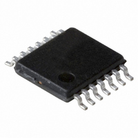
PCA9543CPW,118 NXP Semiconductors, PCA9543CPW,118 Datasheet - Page 8

PCA9543CPW,118
Manufacturer Part Number
PCA9543CPW,118
Description
IC I2C SWITCH 2CH 14-TSSOP
Manufacturer
NXP Semiconductors
Datasheet
1.PCA9543BPW118.pdf
(23 pages)
Specifications of PCA9543CPW,118
Package / Case
14-TSSOP
Applications
2-Channel I²C Multiplexer
Interface
I²C
Voltage - Supply
2.3 V ~ 3.6 V, 4.5 V ~ 5.5 V
Mounting Type
Surface Mount
Product
Multiplexer
Number Of Lines (input / Output)
2.0 / 1.0
Propagation Delay Time
0.3 ns at 2.3 V to 5.5 V
Supply Voltage (max)
5.5 V
Supply Voltage (min)
2.3 V
Maximum Operating Temperature
+ 85 C
Minimum Operating Temperature
- 40 C
Mounting Style
SMD/SMT
Number Of Input Lines
2.0
Number Of Output Lines
1.0
Lead Free Status / RoHS Status
Lead free / RoHS Compliant
For Use With
OM6285 - EVAL BOARD I2C-2002-1A568-4002 - DEMO BOARD I2C
Lead Free Status / Rohs Status
Lead free / RoHS Compliant
Other names
935283306118
PCA9543CPW-T
PCA9543CPW-T
PCA9543CPW-T
PCA9543CPW-T
NXP Semiconductors
7. Characteristics of the I
PCA9543A_43B_43C_6
Product data sheet
7.1 Bit transfer
7.2 START and STOP conditions
Figure
3.5 V or lower, so the PCA9543A supply voltage could be set to 3.3 V. Pull-up resistors
can then be used to bring the bus voltages to their appropriate levels (see
More Information can be found in Application Note AN262: PCA954X family of I
multiplexers and switches .
The I
lines are a serial data line (SDA) and a serial clock line (SCL). Both lines must be
connected to a positive supply via a pull-up resistor when connected to the output stages
of a device. Data transfer may be initiated only when the bus is not busy.
One data bit is transferred during each clock pulse. The data on the SDA line must remain
stable during the HIGH period of the clock pulse as changes in the data line at this time
will be interpreted as control signals (see
Both data and clock lines remain HIGH when the bus is not busy. A HIGH-to-LOW
transition of the data line while the clock is HIGH is defined as the START condition (S). A
LOW-to-HIGH transition of the data line while the clock is HIGH is defined as the STOP
condition (P) (see
Fig 9.
Fig 10. Definition of START and STOP conditions
2
C-bus is for 2-way, 2-line communication between different ICs or modules. The two
8, we see that V
SDA
SCL
Bit transfer
START condition
2
SDA
SCL
Figure
C-bus
S
o(sw)(max)
Rev. 06 — 15 June 2009
10).
2-channel I
will be at 2.7 V when the PCA9543A supply voltage is
data valid
data line
stable;
Figure
2
C-bus switch with interrupt logic and reset
allowed
change
of data
PCA9543A/43B/43C
9).
STOP condition
mba607
P
© NXP B.V. 2009. All rights reserved.
Figure
mba608
2
C/SMBus
15).
8 of 23


