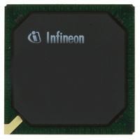
PXB4220E-V32 Infineon Technologies, PXB4220E-V32 Datasheet - Page 257

PXB4220E-V32
Manufacturer Part Number
PXB4220E-V32
Description
IC CHIPSET 8 E1/T1 LINE 256-BGA
Manufacturer
Infineon Technologies
Datasheet
1.PXB4220E-V33.pdf
(290 pages)
Specifications of PXB4220E-V32
Applications
*
Interface
*
Voltage - Supply
*
Package / Case
256-BGA
Mounting Type
Surface Mount
Lead Free Status / RoHS Status
Contains lead / RoHS non-compliant
Other names
PXB4220E-V32
PXB4220E-V32IN
PXB4220E-V32IN
Available stocks
Company
Part Number
Manufacturer
Quantity
Price
Company:
Part Number:
PXB4220E-V32
Manufacturer:
Infineon
Quantity:
35
Company:
Part Number:
PXB4220E-V32
Manufacturer:
Infineon Technologies
Quantity:
10 000
- Current page: 257 of 290
- Download datasheet (4Mb)
The setup and the hold times are defined with regard to a positive clock edge, see
Figure
Taking the actual used clock frequency into account (e.g. up to the max. frequency), the
corresponding (min. and max.) transmit side “clock to output” propagation delay
specifications can be derived. The timing references (tT5 to tT12) are according
toTable 42
In the following tables, A P (column DIR, Direction) defines a signal from the ATM layer
(transmitter, driver) to the PHY layer (receiver), A P defines a signal from the PHY layer
(transmitter, driver) to the ATM layer (receiver).
Figure 64
Figure 65
Data Sheet
Signal
Clock
Signal
Clock
64.
impedance from clock
to
Table
Setup and hold time definition (single- and multi PHY)
Tri-state timing (multi-PHY, multiple devices only)
signal going low
tT11
45.
input setup to clock input hold from clock
tT5, tT7
impedance to clock
signal going low
tT9
257
tT6, tT8
PXB 4219E, PXB 4220E, PXB 4221E
impedance from clock
signal going high
tT12
Electrical Characteristics
signal going high
impedance to clock
tT10
IWE8, V3.4
2003-01-20
UTOPIA1
UTOPIA2
Related parts for PXB4220E-V32
Image
Part Number
Description
Manufacturer
Datasheet
Request
R

Part Number:
Description:
IC CHIPSET 8 E1/T1 LINE 256-BGA
Manufacturer:
Infineon Technologies
Datasheet:

Part Number:
Description:
Interworking Element for 8 E1/T1 Lines
Manufacturer:
Infineon Technologies AG
Datasheet:

Part Number:
Description:
members of Infineon ATM Chipset
Manufacturer:
Infineon Technologies AG
Datasheet:

Part Number:
Description:
Manufacturer:
Infineon Technologies AG
Datasheet:

Part Number:
Description:
Manufacturer:
Infineon Technologies AG
Datasheet:

Part Number:
Description:
Manufacturer:
Infineon Technologies AG
Datasheet:

Part Number:
Description:
Manufacturer:
Infineon Technologies AG
Datasheet:

Part Number:
Description:
Manufacturer:
Infineon Technologies AG
Datasheet:

Part Number:
Description:
Manufacturer:
Infineon Technologies AG
Datasheet:

Part Number:
Description:
Manufacturer:
Infineon Technologies AG
Datasheet:

Part Number:
Description:
16-bit microcontroller with 2x2 KByte RAM
Manufacturer:
Infineon Technologies AG
Datasheet:

Part Number:
Description:
NPN silicon RF transistor
Manufacturer:
Infineon Technologies AG
Datasheet:

Part Number:
Description:
NPN silicon RF transistor
Manufacturer:
Infineon Technologies AG
Datasheet:

Part Number:
Description:
NPN silicon RF transistor
Manufacturer:
Infineon Technologies AG
Datasheet:

Part Number:
Description:
NPN silicon RF transistor
Manufacturer:
Infineon Technologies AG
Datasheet:


