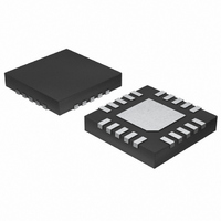
DS8500-JND+ Maxim Integrated Products, DS8500-JND+ Datasheet - Page 4

DS8500-JND+
Manufacturer Part Number
DS8500-JND+
Description
IC MODEM HART SGL 3.6V 20-TQFN
Manufacturer
Maxim Integrated Products
Type
Single Chip Modem with Highway Addressable Remote Transducer (HART) capabilitiesr
Datasheet
1.DS8500-JND.pdf
(7 pages)
Specifications of DS8500-JND+
Applications
HART Modem
Interface
Serial
Voltage - Supply
2.7 V ~ 3.6 V
Package / Case
20-TQFN Exposed Pad
Mounting Type
Surface Mount
Product
HART Modem
Interface Type
Serial
Supply Voltage (max)
3.6 V
Supply Voltage (min)
2.7 V
Supply Current
285 uA
Maximum Operating Temperature
+ 85 C
Minimum Operating Temperature
- 40 C
Mounting Style
SMD/SMT
Data Rate
1.2 Kbps
Number Of Channels
1
Lead Free Status / RoHS Status
Lead free / RoHS Compliant
HART Modem
HART is a backward-compatible enhancement to exist-
ing 4–20mA instrumentation networks that allows two-
way, half-duplex, digital communication with a
microcontroller-based field device. The digital signal is
encoded on top of the existing instrumentation signal.
Communication is accomplished through a series of
commands and responses dependent on the specific
protocol and network topology. The DS8500 does not
implement any portion of the communication protocol; it
only handles the modulation and demodulation of the
encoded information. Digital data is encoded using fre-
quency-shift keying (FSK), which is illustrated in Figure
1. A “1” is identified as a mark symbol and is represent-
ed with a center frequency of 1.2kHz. A “0” is identified
as a space symbol and is represented with a center fre-
quency of 2.2kHz. This allows a throughput of 1.2kbps,
with each symbol occupying an 833µs slot.
Figure 1. HART FSK Signal
The DS8500 modem chip consists of a demodulator, car-
rier detect, digital filter, ADC for input signal conversion, a
modulator and DAC for output signal generation, and
receive and transmit state machine blocks to perform the
HART communication. The Block Diagram illustrates
the interface between various blocks of circuitry.
The input HART signal’s noise interference is attenuat-
ed by a one-pole highpass filter that is external to the
4
V
_______________________________________________________________________________________
1.2kHz MARK
"1"
Functional Description
Introduction to HART
2.2kHz SPACE
"0"
T
chip; the attenuated signal is digitized by the ADC and
filtered by the receive state machine. The transmit state
machine modulates the input to the HART-compliant
signal with the help of the modulator and the DAC.
The modulator performs the FSK modulation of the digi-
tal data at the D_IN input. The FSK-modulated sinu-
soidal signal is present at the FSK_OUT output as
illustrated in Figure 1. The modulator is enabled by RTS
being a logic-low. The modulation is done between
1200Hz (mark) or 2200Hz (space) depending on the
logic level of the input signal. The modulator preserves a
continuous phase when switching between frequencies
to minimize the bandwidth of the transmitted signal.
Figure 2 illustrates an example waveform of the DS8500
in modulate mode. The data to be modulated is pre-
sented in a UART format (start, 8 data bits, parity, stop
bit) at D_IN. FSK_OUT shows the modulated output.
The demodulator accepts an FSK signal at the FSK_IN
input and reproduces the original modulating signal at
the D_OUT output. The HART signal should be present-
ed as an 11-bit UART character with a start, data, pari-
ty, and stop bits for proper operation of the
demodulator block. The nominal bit rate of the D_OUT
signal is 1200 bits per second. A simple RC filter is suf-
ficient for anti-aliasing. Figure 3 illustrates an example
waveform of the DS8500 in demodulate mode.
Figure 4 shows the typical application circuit. As the
DS8500 integrates a digital filter, only a simple passive
RC filter is required in front of the ADC. R3 and C3
implement a lowpass filter with a 10kHz cutoff frequen-
cy; C2 and R2/R1 implement a highpass filter with a
480Hz cutoff frequency. The resistor-divider formed by
R1 and R2 provides an input bias voltage of V
the ADC input (R1 = R2).
The output DAC provides a sine-wave signal, and C4
provides the AC-coupled signal output from the
DS8500. The typical value of C4 can be anything
greater than 20nF based on the application.
For technical support, go to
ic.com/micro.
Applications Information
Technical Support
http://support.maxim-
Demodulator
Modulator
REF
/2 to


