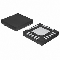
DS8500-JND+ Maxim Integrated Products, DS8500-JND+ Datasheet - Page 2

DS8500-JND+
Manufacturer Part Number
DS8500-JND+
Description
IC MODEM HART SGL 3.6V 20-TQFN
Manufacturer
Maxim Integrated Products
Type
Single Chip Modem with Highway Addressable Remote Transducer (HART) capabilitiesr
Datasheet
1.DS8500-JND.pdf
(7 pages)
Specifications of DS8500-JND+
Applications
HART Modem
Interface
Serial
Voltage - Supply
2.7 V ~ 3.6 V
Package / Case
20-TQFN Exposed Pad
Mounting Type
Surface Mount
Product
HART Modem
Interface Type
Serial
Supply Voltage (max)
3.6 V
Supply Voltage (min)
2.7 V
Supply Current
285 uA
Maximum Operating Temperature
+ 85 C
Minimum Operating Temperature
- 40 C
Mounting Style
SMD/SMT
Data Rate
1.2 Kbps
Number Of Channels
1
Lead Free Status / RoHS Status
Lead free / RoHS Compliant
HART Modem
ABSOLUTE MAXIMUM RATINGS
Voltage Range on All Pins (including AVDD,
Voltage Range on Any Pin Relative to
RECOMMENDED DC OPERATING CONDITIONS
(V
Stresses beyond those listed under “Absolute Maximum Ratings” may cause permanent damage to the device. These are stress ratings only, and functional
operation of the device at these or any other conditions beyond those indicated in the operational sections of the specifications is not implied. Exposure to
absolute maximum rating conditions for extended periods may affect device reliability.
Note 1: Specifications to -40°C are guaranteed by design and are not production tested.
Note 2: Active currents are measured when the device is driven by an external clock XCEN = 1 condition.
Note 3: Guaranteed by design and not production tested.
Note 4: Accuracy is guaranteed based on the external crystal or clock provided.
2
Digital Supply Voltage
Analog Supply Voltage
Ground
Digital Power-Fail Reset Voltage
Active Current
Input Low Voltage
Input High Voltage
Output Low Voltage
Output High Voltage
I/O Pin Capacitance
Input Leakage Current XTAL,
Input Leakage Current All Other
Pins
Input Low Current for
CLOCK SOURCE
External Clock Frequency
VOLTAGE REFERENCE
Internal Reference Voltage
FSK INPUT
Input Voltage Range at FSK_IN
FSK OUTPUT
Output Voltage at FSK_OUT
Frequency of FSK_OUT (Note 4)
DVDD) Relative to Ground .................................-0.5V to +3.6V
Ground Except AVDD, DVDD .............-0.5V to (V
DVDD
_______________________________________________________________________________________
Pullup Resistance
= V
PARAMETER
AVDD
= 2.7V to 3.6V, T
A
= -40°C to +85°C.) (Note 1)
SYMBOL
V
V
R
V
GND
V
I
f
V
V
DVDD
AVDD
V
C
HFIN
I
ILRX
I
V
V
OUT
RST
RST
I
REF
DD
IL1
OH
OL
IL
IO
IL
IL
V
AGND = DGND
Monitors V
V
I
I
Guaranteed by design (Note 3)
V
AC-coupled max 30k
For a mark
For a space
DVDD
OL
OH
AVDD
AVDD
IN
= 4mA
= 0.4V
= -4mA
+ 0.5V)
= V
= V
DVDD
DVDD
DVDD
CONDITIONS
= 2.7V (Note 2)
Operating Temperature Range ...........................-40°C to +85°C
Storage Temperature Range .............................-65°C to +150°C
Soldering Temperature...........................Refer to the IPC/JEDEC
load
DGND
0.75 x
V
DGND
V
0.8 x
2.59
MIN
DVDD
DVDD
-1%
-1%
-1%
400
-30
2.7
2.7
19
-2
0
0
3.6864
1200
2200
TYP
2.64
1.23
500
J-STD-020 Specification.
V
0.30 x
V
MAX
+1%
V
+1%
+1%
2.69
+30
285
DVDD
DVDD
170
600
3.6
3.6
0.4
+2
15
45
REF
0
UNITS
mV
MHz
k
μA
pF
μA
μA
μA
Hz
V
V
V
V
V
V
V
V
V
V
P-P


