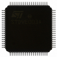
STDVE003ABTR STMicroelectronics, STDVE003ABTR Datasheet - Page 10

STDVE003ABTR
Manufacturer Part Number
STDVE003ABTR
Description
IC EQUALIZER TMDS/HDMI 80-TQFP
Manufacturer
STMicroelectronics
Datasheet
1.STDVE003ABTR.pdf
(42 pages)
Specifications of STDVE003ABTR
Applications
Signal Processing
Interface
I²C
Voltage - Supply
3.135 V ~ 3.465 V
Package / Case
80-TQFP, 80-VQFP
Mounting Type
Surface Mount
For Use With
497-8371 - BOARD EVAL HDMI $ VIDEO SWITCH
Lead Free Status / RoHS Status
Lead free / RoHS Compliant
Other names
497-6838-2
Available stocks
Company
Part Number
Manufacturer
Quantity
Price
Company:
Part Number:
STDVE003ABTR
Manufacturer:
LT
Quantity:
643
Company:
Part Number:
STDVE003ABTR
Manufacturer:
STMicroelectronics
Quantity:
10 000
Part Number:
STDVE003ABTR
Manufacturer:
ST
Quantity:
20 000
Functional description
3
3.1
10/42
Functional description
The STDVE003A routes physical layer signals for high bandwidth digital video and is
compatible with low voltage differential signaling standard like TMDS. The device passes the
differential inputs from a video source to a common display when it is in the active mode of
operation. The device conforms to the TMDS standard on both inputs and outputs.
The low on-resistance and low I/O capacitance of the switch in STDVE003A result in a very
small propagation delay. The device integrates SPDT-type switches for 3 differential data
TMDS channels and 1 differential clock channel. Additionally, it integrates the switches for
DDC and HPD line switching with I
The I
and the hot plug detector (HPD) of the selected input port is output to HPD_SINK. For the
unused ports, the I
Adaptive equalizer
The equalizer dramatically reduces the intersymbol interference (ISI) jitter and attenuation
from long or lossy transmission media. The inputs present high impedance when the device
is not active or when V
on input channels are present.
This circuit helps to improve the signal eye pattern significantly. Shaping is performed by the
gain stage of the equalizer to compensate the signal degradation and then the signals are
driven on to the output ports.
The equalizer is fully adaptive and automatic in function providing smaller gain at low
frequencies and higher gain at high frequencies. The default setting of EQ_BOOST = L is
recommended for optimized operation.
Table 3.
2
C interface of the selected input port is linked to the I
Frequency
(MHz)
Gain frequency response
1650
225
325
410
825
2
C interfaces are isolated and the HPD pins are driven to L state.
CC
is absent or 0 V. In all other cases, the 50
2
C repeater on the DDC lines.
(EQ_BOOST = 0)
Gain in dB
6.5
11
16
3
5
2
C interface of the output port,
Ω
(EQ_BOOST = 1)
termination resistors
Gain in dB
21.5
6.5
8.5
11
16
STDVE003A


