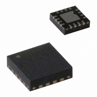
PCA9541BS/03,118 NXP Semiconductors, PCA9541BS/03,118 Datasheet - Page 6

PCA9541BS/03,118
Manufacturer Part Number
PCA9541BS/03,118
Description
IC I2C 2:1 SELECTOR 16-HVQFN
Manufacturer
NXP Semiconductors
Datasheet
1.PCA9541BS03118.pdf
(41 pages)
Specifications of PCA9541BS/03,118
Package / Case
16-VQFN Exposed Pad, 16-HVQFN, 16-SQFN, 16-DHVQFN
Applications
2-Channel I²C Multiplexer
Interface
I²C
Voltage - Supply
2.3 V ~ 3.6 V, 4.5 V ~ 5.5 V
Mounting Type
Surface Mount
Logic Family
PCA
Propagation Delay Time
0.3 ns
Operating Supply Voltage
2.3 V to 3.6 V
Power Dissipation
400 mW
Operating Temperature Range
- 40 C to + 85 C
Mounting Style
SMD/SMT
Output Current
25 mA
Lead Free Status / RoHS Status
Lead free / RoHS Compliant
Lead Free Status / RoHS Status
Lead free / RoHS Compliant, Lead free / RoHS Compliant
Other names
568-1848-2
935273318118
PCA9541BS/03-T
935273318118
PCA9541BS/03-T
NXP Semiconductors
PCA9541_7
Product data sheet
7.2 Pin description
Table 3.
[1]
Symbol
INT0
SDA_MST0
SCL_MST0
RESET
SCL_MST1
SDA_MST1
INT1
V
A0
A1
A2
A3
SCL_SLAVE
SDA_SLAVE
INT_IN
V
SS
DD
HVQFN16 package die supply ground is connected to both the V
V
and board-level performance, the exposed pad needs to be soldered to the board using a corresponding
thermal pad on the board, and for proper heat conduction through the board thermal vias need to be
incorporated in the printed-circuit board in the thermal pad region.
SS
pin must be connected to supply ground for proper device operation. For enhanced thermal, electrical,
Pin description
Pin
SO16,
TSSOP16
1
2
3
4
5
6
7
8
9
10
11
12
13
14
15
16
Rev. 07 — 2 July 2009
2-to-1 I
HVQFN16
15
16
1
2
3
4
5
6
7
8
9
10
11
12
13
14
[1]
2
C-bus master selector with interrupt logic and reset
Description
active LOW interrupt output 0 (external pull-up required)
serial data master 0 (external pull-up required)
serial clock master 0 (external pull-up required)
active LOW reset input (external pull-up required)
serial clock master 1 (external pull-up required)
serial data master 1 (external pull-up required)
active LOW interrupt output 1 (external pull-up required)
supply ground
address input 0 (externally held to V
address input 1 (externally held to V
address input 2 (externally held to V
address input 3 (externally held to V
serial clock slave (external pull-up required)
serial data slave (external pull-up required)
active LOW interrupt input (external pull-up required)
supply voltage
SS
pin and the exposed center pad. The
PCA9541
SS
SS
SS
SS
© NXP B.V. 2009. All rights reserved.
or V
or V
or V
or V
DD
DD
DD
DD
)
)
)
)
6 of 41


