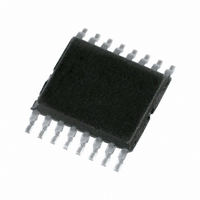
PCA9546APW,112 NXP Semiconductors, PCA9546APW,112 Datasheet - Page 7

PCA9546APW,112
Manufacturer Part Number
PCA9546APW,112
Description
IC I2C SWITCH 4CH 16TSSOP
Manufacturer
NXP Semiconductors
Datasheet
1.PCA9546ABS118.pdf
(25 pages)
Specifications of PCA9546APW,112
Package / Case
16-TSSOP
Applications
4-Channel I²C Switcher
Interface
I²C, SMBus
Voltage - Supply
2.3 V ~ 5.5 V
Mounting Type
Surface Mount
Product
Multiplexer
Number Of Lines (input / Output)
4.0 / 1.0
Propagation Delay Time
0.3 ns
Supply Voltage (max)
3.6 V
Supply Voltage (min)
2.3 V
Maximum Operating Temperature
+ 85 C
Minimum Operating Temperature
- 40 C
Mounting Style
SMD/SMT
Number Of Input Lines
4.0
Number Of Output Lines
1.0
Power Dissipation
400 mW
Lead Free Status / RoHS Status
Lead free / RoHS Compliant
Lead Free Status / RoHS Status
Lead free / RoHS Compliant, Lead free / RoHS Compliant
Other names
568-5026
935275813112
PCA9546APW
PCA9546APW,112
PCA9546APW
935275813112
PCA9546APW
PCA9546APW,112
PCA9546APW
NXP Semiconductors
PCA9546A_5
Product data sheet
6.3 RESET input
6.4 Power-on reset
6.5 Voltage translation
The RESET input is an active LOW signal which may be used to recover from a bus fault
condition. By asserting this signal LOW for a minimum of t
its registers and I
must be connected to V
When power is applied to V
a reset condition until V
and the PCA9546A registers and I
states (all zeroes) causing all the channels to be deselected. Thereafter, V
lowered below 0.2 V to reset the device.
The pass gate transistors of the PCA9546A are constructed such that the V
be used to limit the maximum voltage that will be passed from one I
Figure 7
was generated using the data specified in
sheet). In order for the PCA9546A to act as a voltage translator, the V
be equal to, or lower than the lowest bus voltage. For example, if the main bus was
running at 5 V, and the downstream buses were 3.3 V and 2.7 V, then V
equal to or below 2.7 V to effectively clamp the downstream bus voltages. Looking at
Figure
3.5 V or lower, so the PCA9546A supply voltage could be set to 3.3 V. Pull-up resistors
can then be used to bring the bus voltages to their appropriate levels (see
Fig 7.
(1) maximum
(2) typical
(3) minimum
7, we see that V
shows the voltage characteristics of the pass gate transistors (note that the graph
Pass gate voltage versus supply voltage
2
C-bus state machine and will deselect all channels. The RESET input
V
o(sw)
(V)
o(sw)(max)
DD
5.0
4.0
3.0
2.0
1.0
DD
Rev. 05 — 2 July 2009
2.0
has reached V
through a pull-up resistor.
DD
, an internal Power-On Reset (POR) holds the PCA9546A in
2.5
will be at 2.7 V when the PCA9546A supply voltage is
2
C-bus state machine are initialized to their default
3.0
POR
3.5
Section 10 “Static characteristics”
. At this point, the reset condition is released
4.0
(1)
(2)
(3)
4.5
4-channel I
002aaa964
5.0
V
w(rst)L
DD
(V)
5.5
, the PCA9546A will reset
2
C-bus switch with reset
PCA9546A
2
C-bus to another.
o(sw)
© NXP B.V. 2009. All rights reserved.
o(sw)
DD
voltage should
Figure
DD
should be
of this data
must be
voltage can
14).
7 of 25


