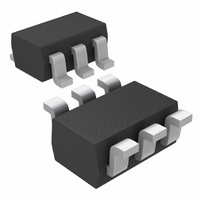
MAX9180EXT+T Maxim Integrated Products, MAX9180EXT+T Datasheet - Page 2

MAX9180EXT+T
Manufacturer Part Number
MAX9180EXT+T
Description
IC REPEATER LVDS SC70-6
Manufacturer
Maxim Integrated Products
Type
Repeaterr
Datasheet
1.MAX9180EXTT.pdf
(9 pages)
Specifications of MAX9180EXT+T
Tx/rx Type
LVDS
Delay Time
2.0ns
Voltage - Supply
3 V ~ 3.6 V
Current - Supply
10mA
Mounting Type
Surface Mount
Package / Case
SC-70-6, SC-88, SOT-363
Lead Free Status / RoHS Status
Lead free / RoHS Compliant
Capacitance - Input
-
ABSOLUTE MAXIMUM RATINGS
V
IN+, IN- to GND.....................................................-0.3V to +4.0V
OUT+, OUT- to GND .............................................-0.3V to +4.0V
Short-Circuit Duration (OUT+, OUT-) .........................Continuous
Continuous Power Dissipation (T
400Mbps, Low-Jitter, Low-Noise LVDS
Repeater in an SC70 Package
Stresses beyond those listed under “Absolute Maximum Ratings” may cause permanent damage to the device. These are stress ratings only, and functional
operation of the device at these or any other conditions beyond those indicated in the operational sections of the specifications is not implied. Exposure to
absolute maximum rating conditions for extended periods may affect device reliability.
DC ELECTRICAL CHARACTERISTICS
(V
noted. Typical values are at V
2
CC
LVDS INPUT
Differential Input High Threshold
Differential Input Low Threshold
Input Current
Power-Off Input Current
Input Resistor 1
Input Resistor 2
LVDS OUTPUT
Differential Output Voltage
Change in V
Complementary Output States
Offset (Common-Mode) Voltage
Change in V
Complementary Output States
Output High Voltage
Output Low Voltage
Fail-Safe Differential Output
Voltage
Power-Off Output Leakage
Current
Differential Output Resistance
Output Short Current
POWER SUPPLY
Supply Current
Supply Current in Fail-Safe
CC
6-Pin SC70 (derate 3.1mW/°C above +70°C) ..............245mW
_______________________________________________________________________________________
to GND ...........................................................-0.3V to +4.0V
= 3.0V to 3.6V, R
PARAMETER
OD
OS
for
Between
L
= 100Ω ±1%,
CC
A
= 3.3V, T
= +70°C)
SYMBOL
I
I
RO
IN+
IN+
|
IO
V
V
R
R
V
V
I
V
V
V
V
I
V
I
CCF
V
OD+
ID
CC
SC
IN1
IN2
OD
OH
A
TH
OS
OL
OFF
TL
DIFF
, I
, I
OD
OS
|
= +25°C.) (Notes 1, 2)
IN-
IN-
= 0.05V to 1.2V, V
0.05V
0.6V <
0.05V
0.6V <
V
V
Figure 2
Figure 2
Figure 2
Figure 2
IN+, IN- shorted, open, or parallel
terminated
V
V
V
V
Output loaded
Output loaded, input undriven
CC
CC
CC
CC
ID
ID
= 50mV, OUT+ = GND
= -50mV, OUT- = GND
= 3.6V or 0V, Figure 1
= 3.6V or 0V, Figure 1
= 0V
= 3.6V or 0V
|
|
V
V
|
|
V
V
ID
ID
ID
ID
|
|
|
|
CM
O U T+ = 3.6V , other outp ut op en
O U T- = 3.6V , other outp ut op en
1.2V
1.2V, V
0.6V
0.6V, V
CONDITIONS
=
|
V
Storage Temperature Range .............................-65°C to +150°C
Junction Temperature ......................................................+150°C
Operating Temperature Range ...........................-40°C to +85°C
ESD Protection
Lead Temperature (soldering, 10s) .................................+300°C
ID
CC
CC
Human Body Model, IN+, IN-, OUT+, OUT- ....................±8kV
/ 2
= 0V
= 0V
|
to 2.4V -
|
V
ID
/ 2
|
, T
A
1.125
+250
= -40°C to +85°C, unless otherwise
MIN
267
250
100
-50
-10
-15
-20
-15
-20
0.9
-10
67
0.008
0.005
+0.02
+0.02
+360
1174
TYP
+1.3
+2.6
1.25
1.44
1.08
-2.5
-3.5
232
360
260
10
-7
-5
-5
7
6
1.375
+450
MAX
+15
+20
+15
+20
+10
+10
450
400
1.6
-15
-15
50
25
25
15
8
U N I T S
mV
mV
mV
mV
mV
mV
mA
mA
mA
µA
µA
k
k
µA
V
V
V


