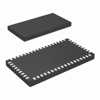
DS50PCI401SQE/NOPB National Semiconductor, DS50PCI401SQE/NOPB Datasheet - Page 4

DS50PCI401SQE/NOPB
Manufacturer Part Number
DS50PCI401SQE/NOPB
Description
IC PCI-E 5GBPS REPEATER 54LLP
Manufacturer
National Semiconductor
Type
Repeaterr
Datasheet
1.DS50PCI401SQENOPB.pdf
(30 pages)
Specifications of DS50PCI401SQE/NOPB
Tx/rx Type
CML/LPDS
Delay Time
200ps
Capacitance - Input
10pF
Voltage - Supply
2.375 V ~ 2.625 V
Mounting Type
Surface Mount
Package / Case
*
Lead Free Status / RoHS Status
Lead free / RoHS Compliant
Current - Supply
-
Other names
DS50PCI401SQETR
Available stocks
Company
Part Number
Manufacturer
Quantity
Price
Company:
Part Number:
DS50PCI401SQE/NOPB
Manufacturer:
TI
Quantity:
38
www.national.com
Pin Descriptions
Pin Name
Differential High Speed I/O's
IA_0+, IA_0- ,
IA_1+, IA_1-,
IA_2+, IA_2-,
IA_3+, IA_3-
OA_0+, OA_0-,
OA_1+, OA_1-,
OA_2+, OA_2-,
OA_3+, OA_3-
IB_0+, IB_0- ,
IB_1+, IB_1-,
IB_2+, IB_2-,
IB_3+, IB_3-
OB_0+, OB_0-,
OB_1+, OB_1-,
OB_2+, OB_2-,
OB_3+, OB_3-
Control Pins — Shared (LVCMOS)
ENSMB
ENSMB = 1 (SMBUS MODE)
SCL
SDA
AD0-AD3
ENSMB = 0 (NORMAL PIN MODE)
EQA0, EQA1
EQB0, EQB1
Pin Number
10, 11
12, 13
15, 16
17, 18
35, 34
33, 32
31, 30
29, 28
45, 44
43, 42
40, 39
38, 37
1, 2
3, 4
5, 6
7, 8
48
50
49
54, 53, 47, 46 I, LVCMOS w/
20, 19
46, 47
I/O, Type
I, CML
O,LPDS
I, CML
O,LPDS
I, LVCMOS w/
internal
pulldown
I, LVCMOS
I, LVCMOS,
O, Open
Drain
internal
pulldown
I,FLOAT,
LVCMOS
Pin Description
Inverting and non-inverting CML differential inputs to the
equalizer. A gated on-chip 50Ω termination resistor connects
INA_0+ to VDD and INA_0- to VDD when enabled.
Inverting and non-inverting low power differential signal
(LPDS) 50Ω driver outputs with de-emphasis. Compatible
with AC coupled CML inputs.
Inverting and non-inverting CML differential inputs to the
equalizer. A gated on-chip 50Ω termination resistor connects
INB_0+ to VDD and INB_0- to VDD when enabled.
Inverting and non-inverting low power differential signal
(LPDS) 50Ω driver outputs with de-emphasis. Compatible
with AC coupled CML inputs.
System Management Bus (SMBus) enable pin.
When pulled high provide access internal digital registers that
are a means of auxiliary control for such functions as
equalization, de-emphasis, VOD, rate, and idle detection
threshold.
When pulled low, access to the SMBus registers are disabled
and SMBus function pins are used to control the Equalizer
and De-Emphasis.
Please refer to “SMBus configuration Registers” section and
Electrical Characteristics - Serial Management Bus Interface
for detail information.
ENSMB = 1
SMBUS clock input pin is enabled. External pull-up resistor
maybe needed. Refer to R
ENSMB = 1
The SMBus bi-directional SDA pin is enabled. Data input or
open drain output. External pull-up resistor is required.
Refer to R
ENSMB = 1
SMBus Slave Address Inputs. In SMBus mode, these pins are
the user set SMBus slave address inputs. See section —
System Management Bus (SMBus) and Configuration
Registers for additional information.
EQA/B ,0/1 controls the level of equalization of the A/B sides
as shown in
ENSMB is de-asserted (Low). Each of the 4 A/B channels
have the same level unless controlled by the SMBus control
registers. When ENSMB goes high the SMBus registers
provide independent control of each lane, and the EQB0/B1
pins are converted to SMBUS AD2/AD3 inputs.
4
TERM
Table
in the SMBus specification.
1. The EQA/B pins are active only when
TERM
in the SMBus specification.


