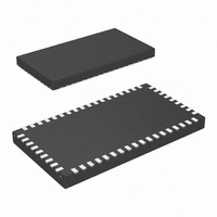
DS50PCI401SQE/NOPB National Semiconductor, DS50PCI401SQE/NOPB Datasheet - Page 12

DS50PCI401SQE/NOPB
Manufacturer Part Number
DS50PCI401SQE/NOPB
Description
IC PCI-E 5GBPS REPEATER 54LLP
Manufacturer
National Semiconductor
Type
Repeaterr
Datasheet
1.DS50PCI401SQENOPB.pdf
(30 pages)
Specifications of DS50PCI401SQE/NOPB
Tx/rx Type
CML/LPDS
Delay Time
200ps
Capacitance - Input
10pF
Voltage - Supply
2.375 V ~ 2.625 V
Mounting Type
Surface Mount
Package / Case
*
Lead Free Status / RoHS Status
Lead free / RoHS Compliant
Current - Supply
-
Other names
DS50PCI401SQETR
Available stocks
Company
Part Number
Manufacturer
Quantity
Price
Company:
Part Number:
DS50PCI401SQE/NOPB
Manufacturer:
TI
Quantity:
38
www.national.com
DE-EMPHASIS
DJD1
DJD2
DJD3
DJD4
Note 1: “Absolute Maximum Ratings” indicate limits beyond which damage to the device may occur, including inoperability and degradation of device reliability
and/or performance. Functional operation of the device and/or non-degradation at the Absolute Maximum Ratings or other conditions beyond those indicated in
the Recommended Operating Conditions is not implied. The Recommended Operating Conditions indicate conditions at which the device is functional and the
device should not be operated beyond such conditions. Absolute Maximum Numbers are guaranteed for a junction temperature range of -40°C to +125°C. Models
are validated to Maximum Operating Voltages only.
Note 2: Typical values represent most likely parametric norms at V
characterization and are not guaranteed.
Note 3: The Electrical Characteristics tables list guaranteed specifications under the listed Recommended Operating Conditions except as otherwise modified
or specified by the Electrical Characteristics Conditions and/or Notes. Typical specifications are estimations only and are not guaranteed.
Note 4: Allowed supply noise (mV
Note 5: Input Return Loss also uses the setup shown in
emulate a typical PCIe application.
Note 6: PCIe 2.0 transmit jitter specifications - actual device jitter is much less. Actual device Rj and Dj has been characterized and specified with test loads
outlined in the EQUALIZATION and DE-EMPHASIS sections of the Electrical Characteristics table.
Note 7: Guaranteed by device characterization
Note 8: Propagation Delay measurements for Part to Part skew are all based on devices operating under indentical temperature and supply voltage conditions.
Note 9: Propagation Delay measurements will change slightly based on the level of EQ selected. EQ Bypass will result in the shortest propagation delays.
Note 10: Residual DJ measurements subtract out deterministic jitter present at the generator outputs. For 2.5 Gbps generator Dj = 0.0275 UI and for 5.0 Gbps
generator Dj = 0.035 UI.
Note 11: Measured with a repeating K28.5 pattern at a data rate of 2.5 Gbps and 5.0 Gbps.
Note 12: Measured with DEM Select pins configured for 1000mV VOD, see De-emphasis table.
Note 13: Measured at default SD_TH settings
Note 14: Input edge rate for LVCMOS/FLOAT inputs must be 50ns minimum from 10-90%.
Note 15: Measured at package pins of receiver. Less than 40mV is IDLE, greater than 175mV is ACTIVE. SD_TH pin connected with resistor to GND overrides
this default setting.
Symbol
Residual Deterministic
Jitter at 5 Gbps
Residual Deterministic
Jitter at 2.5 Gbps
Residual Deterministic
Jitter at 5 Gbps
Residual Deterministic
Jitter at 2.5 Gbps
P-P
Parameter
sine wave) under typical conditions.
Figure
28” of 5 mil stripline FR4,
EQ1,0=F,F; K28.5 pattern,
DEM1,0=F,1; Tx Launch
Amplitude 1.0 Vp-p, SD_TH=F.
(Note
28” of 5 mil microstrip FR4,
EQ1,0=F,F; K28.5 pattern,
DEM1,0=F,0; Tx Launch
Amplitude 1.0 Vp-p, SD_TH=F.
(Note
7 meters of 24 AWG PCIe cable,
EQ1,0=F,F; K28.5 pattern,
DEM1,0=F,1; Tx Launch
Amplitude 1.0 Vp-p, SD_TH=F.
(Note
7 meters of 24 AWG PCIe cable,
EQ1,0=F,F; K28.5 pattern,
DEM1,0=F,0; Tx Launch
Amplitude 1.0 Vp-p, SD_TH=F.
(Note
6. The blocking / biasing circuit is replaced with a simple AC coupling capacitor for each input to
DD
2,
2,
2,
2,
= 2.5V, T
Note
Note
Note
Note
Conditions
10)
10)
10)
10)
12
A
= 25°C., and at the Recommended Operation Conditions at the time of product
Min
0.02
0.03
0.03
0.04
Typ
Max
0.09
0.05
0.13
0.06
Units
UI
UI
UI
UI
P-P
P-P
P-P
P-P


