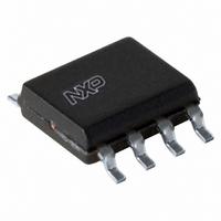
P82B715TD,112 NXP Semiconductors, P82B715TD,112 Datasheet - Page 7

P82B715TD,112
Manufacturer Part Number
P82B715TD,112
Description
IC I2C BUS EXTENDER 8-SOIC
Manufacturer
NXP Semiconductors
Type
Bus Extenderr
Datasheet
1.P82B715TD118.pdf
(23 pages)
Specifications of P82B715TD,112
Package / Case
8-SOIC (3.9mm Width)
Tx/rx Type
I²C Logic
Delay Time
250ns
Capacitance - Input
3000pF
Voltage - Supply
4.5 V ~ 12 V
Current - Supply
22mA
Mounting Type
Surface Mount
Logic Family
P82B
Number Of Lines (input / Output)
1 / 1
Propagation Delay Time
250 ns
Operating Supply Voltage
4.5 V to 12 V
Power Dissipation
300 mW
Operating Temperature Range
- 40 C to + 85 C
Logic Type
I2C Bus Extender
Mounting Style
SMD/SMT
Number Of Input Lines
1
Number Of Output Lines
1
Output Current
60 mA
Lead Free Status / RoHS Status
Lead free / RoHS Compliant
Lead Free Status / RoHS Status
Lead free / RoHS Compliant, Lead free / RoHS Compliant
Other names
568-3981-5
935154770112
P82B715TD
P82B715TD
935154770112
P82B715TD
P82B715TD
Available stocks
Company
Part Number
Manufacturer
Quantity
Price
Company:
Part Number:
P82B715TD,112
Manufacturer:
CIRRUS
Quantity:
130
NXP Semiconductors
P82B715_8
Product data sheet
8.1.2 Calculating static bus drive currents
This equivalent capacitance is the sum of the capacitance on the buffered bus plus
10 times the sum of the capacitances on all the connected I
value should not exceed 4 nF. The single buffered bus pull-up resistor is then calculated to
achieve the rise time requirement and it then provides the pull-up for the buffered bus and
for all other connected I
Figure 6
bus capacitances are omitted for clarity and we assume the pull-up resistors have been
selected to give RC products equal to the bus rise time requirement. An I
connected at I
local pull-up R1 plus, with assistance from the P82B715, the currents in R2, R3 and R4.
When I
I
pins (which are LOW) so their buffer amplifiers will be inactive. The SDA at Sx of I
and I
to Sx. So the effective current that must be sunk by the P82B715 buffer on I
Lx pin, is the sum of the currents in R2, R3 and R4. The Sx current that must be sunk by
an I
effective pull-up, determining the current to be sunk by an I
in parallel with resistors 10 times the values of R2, R3 and R4. If R1 = R3 = R4 = 10 k ,
and R2 = 1 k , the effective pull-up load at I
10 k
The same calculation applies for I
To calculate the current sunk by the Lx pin of the buffer at I
in R1 is sunk directly by the IC at I
flowing in R2, R3, and R4 so the effective pull-up is R2 in parallel with R3 and R4.
In this example that is 1 k
that means the buffer is sinking 16.3 mA.
2
Fig 6.
C-bus 3, and their corresponding Sx pins, to a voltage higher than the voltage at their Lx
I
2
2
C-bus 1
C-bus chip at I
2
C-bus 3 is pulled LOW by the LOW at Lx via the internal 30
V
2
CC
C-bus 1 is LOW, the resistors R3 and R4 act to pull the bus nodes I
10 k
shows three P82B715s connected to a common buffered bus. The associated
Single pull-up on buffered bus and multiple pull-up option
= 5 V
SDA
SCL
2
C-bus 1 and holding the SDA bus LOW must sink the current flowing in its
100 k
2
R1
C-bus 1, due to the buffer gain action, is
Rev. 08 — 9 November 2009
2
Sx
Sy
C-bus nodes included in the calculation.
100 k = 4.55 k . (‘ ’ means ‘in parallel with’.)
10 k
Lx
Ly
2
2
C-bus 2 or I
C-bus 1. The buffer therefore sinks only the currents
buffered bus
10 k = 833 . For a 5.5 V supply and 0.4 V LOW,
R2
2
C-bus 1 is
2
C-bus 3.
Lx
Lx
Ly
Ly
Sx
Sx
2
Sy
Sy
2
2
C-bus chip at I
C-bus 1, note that the current
C-bus nodes. The calculated
1
10
of the Lx current. So the
R3
R4
resistor that links Lx
V
P82B715
CC
© NXP B.V. 2009. All rights reserved.
I
2
2
C-bus extender
= 5 V
2
C-bus chip
2
C-bus 1, is R1
C-bus 1, at its
2
SDA
SCL
SDA
SCL
C-bus 2 and
002aad691
I
I
2
2
2
C-bus 2
C-bus 3
C-bus 2
7 of 23


