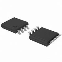
PCA9515DP,118 NXP Semiconductors, PCA9515DP,118 Datasheet - Page 4

PCA9515DP,118
Manufacturer Part Number
PCA9515DP,118
Description
IC I2C BUS REPEATER 8-TSSOP
Manufacturer
NXP Semiconductors
Type
Repeaterr
Datasheet
1.PCA9515DP118.pdf
(16 pages)
Specifications of PCA9515DP,118
Package / Case
8-TSSOP
Tx/rx Type
I²C Logic
Delay Time
55ns
Capacitance - Input
6pF
Voltage - Supply
3 V ~ 3.6 V
Current - Supply
2.3mA
Mounting Type
Surface Mount
Logic Family
PCA9515
Operating Supply Voltage
2.3 V to 3.6 V
Power Dissipation
100 mW
Operating Temperature Range
- 40 C to + 85 C
Input Voltage
5.5 V
Logic Type
I2C Bus
Maximum Clock Frequency
400 KHz
Mounting Style
SMD/SMT
Output Current
50 mA
Output Voltage
5.5 V
Lead Free Status / RoHS Status
Lead free / RoHS Compliant
For Use With
OM6285 - EVAL BOARD I2C-2002-1A568-4002 - DEMO BOARD I2C
Lead Free Status / Rohs Status
Lead free / RoHS Compliant
Other names
568-1034-2
935268635118
PCA9515DP-T
935268635118
PCA9515DP-T
NXP Semiconductors
6. Functional description
PCA9515_9
Product data sheet
6.1 Enable
6.2 I
The PCA9515 BiCMOS integrated circuit contains two identical buffer circuits which
enable I
performance. (Refer to
The PCA9515 BiCMOS integrated circuit contains two bidirectional open-drain buffers
specifically designed to support the standard low-level-contention arbitration of the
I
non-inverting, open-drain buffers, one for SDA and one for SCL.
The EN pin is active HIGH with an internal pull-up and allows the user to select when the
repeater is active. This can be used to isolate a badly behaved slave on power-up until
after the system power-up reset. It should never change state during an I
because disabling during a bus operation will hang the bus and enabling part way through
a bus cycle could confuse the I
The enable pin (EN) should only change state when the global bus and the repeater port
are in an idle state to prevent system failures.
As with the standard I
HIGH levels on the buffered bus. (Standard open-collector configuration of the I
The size of these pull-up resistors depends on the system, but each side of the repeater
must have a pull-up resistor. This part is designed to work with Standard-mode and
Fast-mode I
only specify 3 mA output drive; this limits the termination current to 3 mA in a generic
I
certain conditions, higher termination currents can be used. Please see application note
AN255, “I
resistors and precautions when using more than one PCA9515 in a system or using the
PCA9515 in conjunction with the P82B96.
2
2
2
C-bus. Except during arbitration or clock stretching, the PCA9515 acts like a pair of
C-bus system where Standard-mode devices and multiple masters are possible. Under
C-bus systems
2
C-bus and similar bus systems to be extended without degradation of system
2
C/SMBus Repeaters, Hubs and Expanders” for additional information on sizing
2
C-bus devices in addition to SMBus devices. Standard-mode I
2
C-bus system, pull-up resistors are required to provide the logic
Figure 1 “Block diagram of
Rev. 09 — 23 April 2009
2
C-bus parts being enabled.
PCA9515”.)
PCA9515
© NXP B.V. 2009. All rights reserved.
I
2
2
C-bus operation
C-bus repeater
2
C-bus devices
2
C-bus.)
4 of 16


