MAX3890ECB+D Maxim Integrated Products, MAX3890ECB+D Datasheet - Page 5
MAX3890ECB+D
Manufacturer Part Number
MAX3890ECB+D
Description
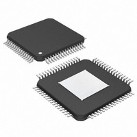
IC 16:1 SERIALIZER 64-TQFP-EP
Manufacturer
Maxim Integrated Products
Datasheet
1.MAX3890ECBD.pdf
(12 pages)
Specifications of MAX3890ECB+D
Function
Serializer
Data Rate
2.5Gbps
Input Type
LVDS
Output Type
PECL
Number Of Inputs
16
Number Of Outputs
1
Voltage - Supply
3 V ~ 3.6 V
Operating Temperature
-40°C ~ 85°C
Mounting Type
Surface Mount
Package / Case
64-TQFP Exposed Pad, 64-eTQFP, 64-HTQFP, 64-VQFP
Lead Free Status / RoHS Status
Lead free / RoHS Compliant


40, 42, 44, 46, 50, 52
41, 43, 45, 47, 51, 53
1, 17, 33, 48, 49, 63
18, 20, 22, 24, 26,
28, 30, 34, 36, 38,
19, 21, 23, 25, 27,
29, 31, 35, 37, 39,
14, 32, 56, 60, 64
2, 5, 7, 10, 13,
PIN
EP
11
12
15
16
54
55
57
58
59
61
62
3
4
6
8
9
+3.3V, 2.5Gbps, SDH/SONET 16:1 Serializer
_______________________________________________________________________________________
with Clock Synthesis and LVDS Inputs
PDI15+ to
PDI15- to
SCLKO+
PCLKO+
Exposed
CLKSET
SCLKO-
PCLKO-
PCLKI+
SLBO+
RCLK+
PCLKI-
NAME
SLBO-
RCLK-
SDO+
PDI0+
SDO-
PDI0-
GND
FIL+
SOS
V
Pad
FIL-
CC
Ground
+3.3V Supply Voltage
System Loopback Inverting Output. Enabled when SOS is high.
System Loopback Noninverting Output. Enabled when SOS is high.
System Loopback Output Select. System loopback disabled when low.
Inverting PECL Serial Clock Output
Noninverting PECL Serial Clock Output
Inverting PECL Serial-Data Output
Noninverting PECL Serial-Data Output
Noninverting LVDS Parallel Clock Input. Connect the incoming parallel-clock signal to the
PCLKI inputs. Note that data is updated on the positive transition of the PCLKI signal.
Inverting LVDS Parallel Clock Input. Connect the incoming parallel-clock signal to the PCLKI
inputs. Note that data is updated on the positive transition of the PCLKI signal.
Noninverting LVDS Parallel Data Inputs. Data is clocked on the PCLKI positive transition.
Inverting LVDS Parallel Data Inputs. Data is clocked on the PCLKI positive transition.
Noninverting LVDS Parallel Clock Output. Use positive transition of PCLKO to clock the
overhead management circuit.
Inverting LVDS Parallel Clock Output. Use positive transition of PCLKO to clock the over-
head management circuit.
Noninverting LVDS Reference Clock Input. Connect an LVDS-compatible crystal refer-
ence clock to the RCLK inputs.
Inverting LVDS Reference Clock Input. Connect an LVDS-compatible crystal reference
clock to the RCLK inputs.
Reference Clock Rate Programming Pin:
CLKSET = V
CLKSET = Open: Reference Clock Rate = 77.76MHz
CLKSET = 20kΩ to GND: Reference Clock Rate = 51.84MHz
CLKSET = GND: Reference Clock Rate = 38.88MHz
Filter Capacitor Input. Connect a 330nF capacitor between FIL+ and FIL-.
Filter Capacitor Input. Connect a 330nF capacitor between FIL+ and FIL-.
Ground. This must be soldered to a circuit board for proper thermal performance (see
Package Information).
CC
: Reference Clock Rate = 155.52MHz
FUNCTION
Pin Description
5
Related parts for MAX3890ECB+D
Image
Part Number
Description
Manufacturer
Datasheet
Request
R

Part Number:
Description:
MAX7528KCWPMaxim Integrated Products [CMOS Dual 8-Bit Buffered Multiplying DACs]
Manufacturer:
Maxim Integrated Products
Datasheet:
Part Number:
Description:
Single +5V, fully integrated, 1.25Gbps laser diode driver.
Manufacturer:
Maxim Integrated Products
Datasheet:
Part Number:
Description:
Single +5V, fully integrated, 155Mbps laser diode driver.
Manufacturer:
Maxim Integrated Products
Datasheet:
Part Number:
Description:
VRD11/VRD10, K8 Rev F 2/3/4-Phase PWM Controllers with Integrated Dual MOSFET Drivers
Manufacturer:
Maxim Integrated Products
Datasheet:
Part Number:
Description:
Highly Integrated Level 2 SMBus Battery Chargers
Manufacturer:
Maxim Integrated Products
Datasheet:
Part Number:
Description:
Current Monitor and Accumulator with Integrated Sense Resistor; ; Temperature Range: -40°C to +85°C
Manufacturer:
Maxim Integrated Products
Part Number:
Description:
TSSOP 14/A�/RS-485 Transceivers with Integrated 100O/120O Termination Resis
Manufacturer:
Maxim Integrated Products
Part Number:
Description:
TSSOP 14/A�/RS-485 Transceivers with Integrated 100O/120O Termination Resis
Manufacturer:
Maxim Integrated Products
Part Number:
Description:
QFN 16/A�/AC-DC and DC-DC Peak-Current-Mode Converters with Integrated Step
Manufacturer:
Maxim Integrated Products
Part Number:
Description:
TDFN/A/65V, 1A, 600KHZ, SYNCHRONOUS STEP-DOWN REGULATOR WITH INTEGRATED SWI
Manufacturer:
Maxim Integrated Products
Part Number:
Description:
Integrated Temperature Controller f
Manufacturer:
Maxim Integrated Products
Part Number:
Description:
SOT23-6/I�/45MHz to 650MHz, Integrated IF VCOs with Differential Output
Manufacturer:
Maxim Integrated Products
Part Number:
Description:
SOT23-6/I�/45MHz to 650MHz, Integrated IF VCOs with Differential Output
Manufacturer:
Maxim Integrated Products
Part Number:
Description:
EVALUATION KIT/2.4GHZ TO 2.5GHZ 802.11G/B RF TRANSCEIVER WITH INTEGRATED PA
Manufacturer:
Maxim Integrated Products
Part Number:
Description:
QFN/E/DUAL PCIE/SATA HIGH SPEED SWITCH WITH INTEGRATED BIAS RESISTOR
Manufacturer:
Maxim Integrated Products
Datasheet: