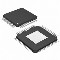
MAX3890ECB+D Maxim Integrated Products, MAX3890ECB+D Datasheet - Page 3

MAX3890ECB+D
Manufacturer Part Number
MAX3890ECB+D
Description
IC 16:1 SERIALIZER 64-TQFP-EP
Manufacturer
Maxim Integrated Products
Datasheet
1.MAX3890ECBD.pdf
(12 pages)
Specifications of MAX3890ECB+D
Function
Serializer
Data Rate
2.5Gbps
Input Type
LVDS
Output Type
PECL
Number Of Inputs
16
Number Of Outputs
1
Voltage - Supply
3 V ~ 3.6 V
Operating Temperature
-40°C ~ 85°C
Mounting Type
Surface Mount
Package / Case
64-TQFP Exposed Pad, 64-eTQFP, 64-HTQFP, 64-VQFP
Lead Free Status / RoHS Status
Lead free / RoHS Compliant
DC ELECTRICAL CHARACTERISTICS (continued)
(V
T
AC ELECTRICAL CHARACTERISTICS
(V
T
Note 1: AC characteristics guaranteed by design and characterization.
Note 2: Setup and hold times are relative to the rising edge of PCLKI+, measured by applying a 155.52MHz differential parallel
Note 3: For f
A
A
Serial Clock Rate
Parallel Data Setup Time
Parallel Data-Hold Time
Output Jitter Generation (SCLKO±)
PROGRAMMING INPUT (CLKSET)
TTL INPUT (SOS)
CURRENT MODE LOGIC (CML) OUTPUTS (SLBO±)
CLKSET Input Current
Input Voltage High
Input Voltage Low
Input Current High
Input Current Low
Differential Output Voltage
Single-Ended Output Resistance
PCLKO to PCLKI Skew
PECL Differential Output Rise/Fall
Time
Parallel Input Clock Rate
Reference Clock Input (RCLKI)
Rise/Fall Time
Parallel Clock Output (PCLKO)
Rise/Fall Time
Serial Clock Output (SCLKO) to
Serial-Data Output (SDO) Delay
CC
CC
= -40°C to +85°C, unless otherwise noted. Typical values are at V
= -40°C to +85°C, unless otherwise noted. Typical values are at V
= +3.0V to +3.6V, differential LVDS loads = 100Ω ±1%, PECL loads = 50Ω ±1% to (V
= +3.0V to +3.6V, differential LVDS load = 100Ω ±1%, PECL loads = 50Ω ±1% to (V
clock with rise/fall time = 1ns (20% to 80%). See Figure 2.
PARAMETER
PARAMETER
RCLK
+3.3V, 2.5Gbps, SDH/SONET 16:1 Serializer
= 38.88MHz, the minimum reference clock amplitude is ≥ 200mV.
_______________________________________________________________________________________
with Clock Synthesis and LVDS Inputs
SYMBOL
t
SCLK-SD
f
t
f
PCLKI
t
t
SYMBOL
SKEW
t
SCLK
R
R
R,
I
t
t
Φ
CLKSET
SU
,
,
H
|V
0
t
V
t
t
V
R
I
F
I
F
F
OD
IH
IL
IH
IL
O
|
20% to 80%, f = 155.52MHz
20% to 80%
SCLKO rising edge to SDO edge
(Note 2)
(Note 2)
Figure 2
Jitter bandwidth = 12kHz to 20MHz,
RCLK amplitude >
20% to 80%
CLKSET = 0 or V
CONDITIONS
CONDITIONS
CC
CC
|
CC
V
= +3.3V, T
= +3.3V, T
IDTH
|
(Note 3)
A
A
= +25°C.) (Note 1)
= +25°C.)
CC
CC
MIN
100
- 2V), CML loads = 50Ω ±1% to V
2.0
-10
-10
- 2V), CML loads = 50Ω ±1% to V
MIN
300
700
110
0
TYP
50
155.52
2.488
TYP
±500
MAX
400
0.8
10
10
MAX
+4.0
120
290
1.0
1.0
3
UNITS
UNITS
ps
mV
µA
µA
µA
GHz
MHz
Ω
V
V
ps
ps
ps
ps
ns
ns
ns
RMS
CC,
CC
3
,


