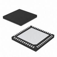
MAX9217ETM+T Maxim Integrated Products, MAX9217ETM+T Datasheet - Page 13

MAX9217ETM+T
Manufacturer Part Number
MAX9217ETM+T
Description
IC SERIALIZER LVDS 48-TQFN
Manufacturer
Maxim Integrated Products
Datasheet
1.MAX9217ETMT.pdf
(15 pages)
Specifications of MAX9217ETM+T
Function
Serializer
Data Rate
700Mbps
Input Type
LVTTL/LVCMOS
Output Type
LVDS
Number Of Inputs
27
Number Of Outputs
1
Voltage - Supply
3 V ~ 3.6 V
Operating Temperature
-40°C ~ 85°C
Mounting Type
Surface Mount
Package / Case
48-TQFN Exposed Pad
Lead Free Status / RoHS Status
Lead free / RoHS Compliant
Driving PWRDWN low stops the PLL, switches out the
integrated 100Ω output termination, and puts the output
in high impedance to ground and differentially. With
PWRDWN ≤ 0.3V and all LVTTL/LVCMOS inputs ≤ 0.3V or
≥ V
Driving PWRDWN high starts PLL lock to PCLK_IN and
switches in the 100Ω output termination resistor. The
LVDS output is not driven until the PLL locks. The LVDS
output is high impedance to ground and 100Ω differen-
tial. The 100Ω integrated termination pulls OUT+ and
OUT- together while the PLL is locking so that V
If V
outputs are high impedance to ground and differentially.
The PLL lock time is set by an internal counter. The lock
time is 16,385 PCLK_IN cycles. Power and clock should
be stable to meet the lock-time specification.
The single-ended inputs (RGB_IN[17:0], CNTL_IN[8:0],
DE_IN, RNG0, RNG1, PCLK_IN, and PWRDWN) are
powered from V
1.71V to 3.6V supply, allowing logic inputs with a nomi-
nal swing of V
when power is applied to V
and PWRDWN is internally driven low, putting the
device in the power-down state.
CC
CCIN
= 0, the output resistor is switched out and the LVDS
- 0.3V, supply current is reduced to 50µA or less.
CCIN
CCIN
______________________________________________________________________________________
. If no power is applied to V
Power-Down and Power-Off
. V
CCIN
CC
Input Buffer Supply
, the inputs are disabled
can be connected to a
PLL Lock Time
OD
DC-Balanced LVDS Serializer
= 0V.
CCIN
The MAX9217 has isolated on-chip power domains. The
digital core supply (V
(V
The PLL has separate power and ground (V
V
power and ground (V
grounds are isolated by diode connections. Bypass each
V
cy, surface-mount ceramic 0.1µF and 0.001µF capacitors
in parallel as close to the device as possible, with the
smallest value capacitor closest to the supply pin.
The LVDS output is a current source. The voltage swing
is proportional to the termination resistance. The output
is rated for a differential load of 100Ω ±1%.
Interconnect for LVDS typically has a differential imped-
ance of 100Ω. Use cables and connectors that have
matched differential impedance to minimize impedance
discontinuities.
Twisted-pair and shielded twisted-pair cables offer
superior signal quality compared to ribbon cable and
tend to generate less EMI due to magnetic field cancel-
ing effects. Balanced cables pick up noise as common
mode, which is rejected by the LVDS receiver.
27-Bit, 3MHz-to-35MHz
CCPLL
CC
CCIN
, V
) are isolated but have a common ground (GND).
CCIN
Power-Supply Circuits and Bypassing
GND) and the LVDS input also has separate
, V
CCPLL
, and V
CC
CCLVDS
) and single-ended input supply
Cables and Connectors
CCLVDS
and V
pin with high-frequen-
CCLVDS
LVDS Output
CCPLL
GND). The
and
13


