LM2502SQX/NOPB National Semiconductor, LM2502SQX/NOPB Datasheet - Page 4
LM2502SQX/NOPB
Manufacturer Part Number
LM2502SQX/NOPB
Description
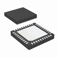
IC SER/DESER MPL DISPL 40-LLP
Manufacturer
National Semiconductor
Series
LMr
Datasheet
1.LM2502SMNOPB.pdf
(27 pages)
Specifications of LM2502SQX/NOPB
Function
Serializer/Deserializer
Data Rate
307Mbps
Input Type
LVCMOS
Output Type
LVCMOS
Number Of Inputs
22
Number Of Outputs
3
Voltage - Supply
1.7 V ~ 3.3 V
Operating Temperature
-30°C ~ 85°C
Mounting Type
Surface Mount
Package / Case
40-LLP
Lead Free Status / RoHS Status
Lead free / RoHS Compliant
Other names
LM2502SQX
Available stocks
Company
Part Number
Manufacturer
Quantity
Price
Company:

Part Number:
LM2502SQX/NOPB
Manufacturer:
NS
Quantity:
2 000


www.national.com
MPL SERIAL BUS PINS
CONFIGURATION/PARALLEL BUS PINS
A/D (RS or
Pin Name
(E or RD*)
PLL_CON
Pin Descriptions
CLKDIS*
(R/W* or
MD[1:0]
D[15:0]
Mode
WR*)
V
CS1*
CS2*
INTR
M/S*
MF0
MF1
CLK
[2:0]
PD*
MC
A0)
SSA
or
of Pins
No.
16
2
1
1
1
1
1
1
1
1
1
1
1
3
I/O, Type
LVCMOS
LVCMOS
LVCMOS
LVCMOS
LVCMOS
LVCMOS
LVCMOS
LVCMOS
LVCMOS
LVCMOS
LVCMOS
LVCMOS
IO, MPL
IO, MPL
Ground
O or I,
IO,
IO,
IO,
IO,
IO,
IO,
IO,
I,
I,
I,
I,
MPL Data Line Driver/Receiver
MPL Clock Line Driver
MPL Ground - see Power/Ground Pins
Master/Slave* Input,
M/S* = H for Master
Power_Down* Input,
H = Active
L = Power Down Mode
Multi-function Input Zero (0):
If MODE = L (m68 mode), E input pin,
data is latched on E High-to-Low
transition or E may be static High and
Data is latched on CS* Low-to-High edge
If MODE = H (i80 mode), Read Enable
input pin, active low. Read data is driven
when both RD* and CS* are Low.
Multi-function Input One (1):
If Mode = L (m68 mode), Read/Write*
pin, Read High, Write* Low
If Mode = H (i80 mode), Write* enable
input pin, active Low. Write data is
latched on the Low-to-High transition of
either WR* or CS* (which ever occurs
first).
ChipSelect1* – Input
H = Ignored
L = Active
ChipSelect2* – Input
H = Ignored
L = Active
Address/Data – Input
H = Data
L = Address (Command)
Data Bus – Inputs/Outputs
INTR is asserted when the read data is
ready and de-asserted upon a second
CPU Read cycle.
Clock Input
Mode Input Pin
H = i80 Mode,
L = m68 Mode
PLL Configuration Input Pins – see Table
10
Master (SER)
4
Description
MPL Data Receiver/Line Driver
MPL Clock Receiver
MPL Ground - see Power/Ground Pins
Master/Slave* Input
M/S* = L for Slave
Power_Down* Input,
H = Active
L = Power Down Mode
Multi-function Output Zero (0):
If MODE = L (m68 mode),
E output pin, static High.
If MODE = H (i80 mode),
Read Enable output pin, active Low.
Multi-function Output One (1):
If Mode = L (m68 mode)
Read/Write* pin,
Read High, Write* Low
If Mode = H (i80 mode)
Write* enable output pin, active Low.
ChipSelect1* – Output
H = Ignored
L = Active
ChipSelect2* – Output
H = Ignored
L = Active
Address/Data – Output
H = Data
L = Address (Command)
Data Bus – Outputs/Inputs
Clock Disable - CLKDIS*:
H = CLK output ON
L = CLK output LOW, allows for the
Slave clock output to be held static if not
used.
Clock Output (Frequency Reference) –
no phase relationship to data – frequency
reference only.
Mode Input Pin
H = i80 Mode,
L = m68 Mode
Clock Divisor Configuration Input Pins –
see Table 10
Slave (DES)
Related parts for LM2502SQX/NOPB
Image
Part Number
Description
Manufacturer
Datasheet
Request
R

Part Number:
Description:
IC SER/DESER MPL DISPL 40-LLP
Manufacturer:
National Semiconductor
Datasheet:

Part Number:
Description:
National Semiconductor [8-Bit D/A Converter]
Manufacturer:
National Semiconductor
Datasheet:
Part Number:
Description:
National Semiconductor [Media Coprocessor]
Manufacturer:
National Semiconductor
Datasheet:
Part Number:
Description:
Digitally Controlled Tone and Volume Circuit with Stereo Audio Power Amplifier, Microphone Preamp Stage and National 3D Sound
Manufacturer:
National Semiconductor
Datasheet:
Part Number:
Description:
Digitally Controlled Tone and Volume Circuit with Stereo Audio Power Amplifier, Microphone Preamp Stage and National 3D Sound
Manufacturer:
National Semiconductor
Datasheet:
Part Number:
Description:
AC97 Rev 2 Codec with Sample Rate Conversion and National 3D Sound
Manufacturer:
National Semiconductor
Part Number:
Description:
Manufacturer:
National Semiconductor
Datasheet:
Part Number:
Description:
Manufacturer:
National Semiconductor
Datasheet:
Part Number:
Description:
General Purpose, Low Voltage, Low Power, Rail-to-Rail Output Operational Amplifiers
Manufacturer:
National Semiconductor
Datasheet:
Part Number:
Description:
8-bit 20 MSPS flash A/D converter.
Manufacturer:
National Semiconductor
Datasheet:
Part Number:
Description:
Low Noise Quad Operational Amplifier
Manufacturer:
National Semiconductor
Datasheet:
Part Number:
Description:
Quad Differential Line Receivers
Manufacturer:
National Semiconductor
Datasheet:
Part Number:
Description:
Quad High Speed Trapezoidal? Bus Transceiver
Manufacturer:
National Semiconductor
Datasheet:
Part Number:
Description:
Dual Line Receiver
Manufacturer:
National Semiconductor
Datasheet: