LM2502SM/NOPB National Semiconductor, LM2502SM/NOPB Datasheet - Page 24
LM2502SM/NOPB
Manufacturer Part Number
LM2502SM/NOPB
Description
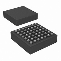
IC SER/DESER MPL DISPL 49-UFBGA
Manufacturer
National Semiconductor
Series
LMr
Datasheet
1.LM2502SMNOPB.pdf
(27 pages)
Specifications of LM2502SM/NOPB
Function
Serializer/Deserializer
Data Rate
307Mbps
Input Type
LVCMOS
Output Type
LVCMOS
Number Of Inputs
22
Number Of Outputs
3
Voltage - Supply
1.7 V ~ 3.3 V
Operating Temperature
-30°C ~ 85°C
Mounting Type
Surface Mount
Package / Case
49-UFBGA
Lead Free Status / RoHS Status
Lead free / RoHS Compliant
Other names
LM2502SMTR
Available stocks
Company
Part Number
Manufacturer
Quantity
Price
Company:

Part Number:
LM2502SM/NOPB
Manufacturer:
Texas Instruments
Quantity:
10 000


www.national.com
Application Information
RGB565 APPLICATION
The LM2502 chipset may also be configured for a RGB565
application. This is also known as a "buffer-less" or "dumb"
display application. In this configuration 16 color bits (R[4:0],
G[5:0], B[4:0]), Pixel Clock (PCLK) and two control bits (VS
and HS) are supported. An external invertor is also required.
To configure for the RGB565 mode, the i80 mode must be
selected. The Pixel clock should be connected to both the
CLK input and the WR* pins on the Master. The PLL_CON
pins should be configured for a 6X mode, as it takes 5 MC
cycles to transfer the RGB data, and the 6X setting will
provide a 50% output PCLK from the Slave device. The 50%
duty cycle PCLK is created by the WR* signal which pulses
low for 3 MC cycles and is high for 2 MC cycles and an idle
MC cycle. See Figure 20 for details. Support is provided for
QVGA Example - For a QVGA display (320 by 240), with 16
bits of color depth and 60 frames per second, a net band-
FIGURE 19. Display Interface Application
(Continued)
FIGURE 20. RGB565 Application
24
PCLKs in the 3 to 12.8 MHz range. PLLCON setting of X8 is
also possible, however, the Slave output PCLK (WR*) will
have some duty cycle distortion (37.5%) and the CLK range
is further restricted.
Slower PCLK rates maybe supported if a higher frequency
multiple of the PCLK is available. For example, if a 2MHz
PCLK is required, then a 6MHz CLK (freq locked, not phase)
may be applied to the MST CLK input and the 2MHz PCLK
to the MST WR* signal input. The PLLCON setting should be
selected as 2X (PLLCON[2:0] = 000’b). Once again 5 MC
cycles are required to transfer the pixel data, and the WR*
(PCLK) will be 50% duty cycle. The applied CLK and
PLLCON should be selected such that is creates a 6X
multiple on MC to ensure a 50% duty cycle.
width requirement is 73.728 Mbps. Maximum transfer rate
20093322
20093301
Related parts for LM2502SM/NOPB
Image
Part Number
Description
Manufacturer
Datasheet
Request
R

Part Number:
Description:
Mobile Pixel Link Mpl Display Interface Serializer And Deserializer
Manufacturer:
National Semiconductor Corporation
Datasheet:

Part Number:
Description:
National Semiconductor [8-Bit D/A Converter]
Manufacturer:
National Semiconductor
Datasheet:
Part Number:
Description:
National Semiconductor [Media Coprocessor]
Manufacturer:
National Semiconductor
Datasheet:
Part Number:
Description:
Digitally Controlled Tone and Volume Circuit with Stereo Audio Power Amplifier, Microphone Preamp Stage and National 3D Sound
Manufacturer:
National Semiconductor
Datasheet:
Part Number:
Description:
Digitally Controlled Tone and Volume Circuit with Stereo Audio Power Amplifier, Microphone Preamp Stage and National 3D Sound
Manufacturer:
National Semiconductor
Datasheet:
Part Number:
Description:
AC97 Rev 2 Codec with Sample Rate Conversion and National 3D Sound
Manufacturer:
National Semiconductor
Part Number:
Description:
Manufacturer:
National Semiconductor
Datasheet:
Part Number:
Description:
Manufacturer:
National Semiconductor
Datasheet:
Part Number:
Description:
General Purpose, Low Voltage, Low Power, Rail-to-Rail Output Operational Amplifiers
Manufacturer:
National Semiconductor
Datasheet:
Part Number:
Description:
8-bit 20 MSPS flash A/D converter.
Manufacturer:
National Semiconductor
Datasheet:
Part Number:
Description:
Low Noise Quad Operational Amplifier
Manufacturer:
National Semiconductor
Datasheet:
Part Number:
Description:
Quad Differential Line Receivers
Manufacturer:
National Semiconductor
Datasheet:
Part Number:
Description:
Quad High Speed Trapezoidal? Bus Transceiver
Manufacturer:
National Semiconductor
Datasheet:
Part Number:
Description:
Dual Line Receiver
Manufacturer:
National Semiconductor
Datasheet: