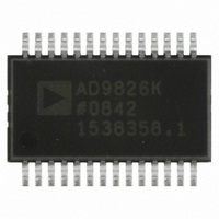
AD9826KRSZ Analog Devices Inc, AD9826KRSZ Datasheet - Page 2

AD9826KRSZ
Manufacturer Part Number
AD9826KRSZ
Description
IC IMAGE SGNL PROC 16BIT 28-SSOP
Manufacturer
Analog Devices Inc
Type
Image Sensorr
Datasheet
1.AD9826KRSZRL.pdf
(20 pages)
Specifications of AD9826KRSZ
Input Type
Logic
Output Type
Logic
Interface
3-Wire Serial
Current - Supply
75mA
Mounting Type
Surface Mount
Package / Case
28-SSOP
Ic Interface Type
Serial
Supply Voltage Range
4.75V To 5.25V, 3V To 5.25V
Power Dissipation Pd
400mW
Operating Temperature Range
-40°C To +85°C
Digital Ic Case Style
SSOP
No. Of Pins
28
Lead Free Status / RoHS Status
Lead free / RoHS Compliant
Available stocks
Company
Part Number
Manufacturer
Quantity
Price
Company:
Part Number:
AD9826KRSZ
Manufacturer:
AD
Quantity:
5 510
Part Number:
AD9826KRSZ
Manufacturer:
ADI/亚德诺
Quantity:
20 000
Part Number:
AD9826KRSZ-REEL
Manufacturer:
ADI/亚德诺
Quantity:
20 000
Company:
Part Number:
AD9826KRSZRL
Manufacturer:
ST
Quantity:
2 904
Part Number:
AD9826KRSZRL
Manufacturer:
ADI/亚德诺
Quantity:
20 000
AD9826–SPECIFICATIONS
ANALOG SPECIFICATIONS
Parameter
MAXIMUM CONVERSION RATE
ACCURACY (ENTIRE SIGNAL PATH)
ANALOG INPUTS
AMPLIFIERS
NOISE AND CROSSTALK
POWER SUPPLY REJECTION
DIFFERENTIAL VREF (at 25 C)
TEMPERATURE RANGE
POWER SUPPLIES
OPERATING CURRENT
POWER DISSIPATION
NOTES
2
Specifications subject to change without notice.
RESET TRANSIENT
The PGA Gain is approximately “linear in dB” and follows the equation:
1
Linear Input Signal Range is from 0 V to 4 V when the CCD’s reference level is clamped to 4 V by the AD9826’s input clamp.
3-Channel Mode with CDS
2-Channel Mode with CDS
1-Channel Mode with CDS
ADC Resolution
Integral Nonlinearity (INL)
Differential Nonlinearity (DNL)
No Missing Codes
Input Signal Range (Programmable)
Allowable Reset Transient
Input Limits
Input Capacitance
Input Bias Current
PGA Gain
PGA Gain Resolution
PGA Gain Monotonicity
Programmable Offset
Programmable Offset Resolution
Programmable Offset Monotonicity
Total Output Noise @ PGA Minimum
Total Output Noise @ PGA Maximum
Channel-to-Channel Crosstalk
AVDD = 5 V
CAPT–CAPB
Operating
Storage
AVDD
DRVDD
AVDD
DRVDD
Power-Down Mode
3-Channel Mode
1-Channel Mode
1V TYP
@ 15 MSPS
@ 6 MSPS
2
0.25 V
2
1
4V SET BY INPUT CLAMP
(3V OPTION ALSO AVAILABLE)
4V p-p MAX INPUT SIGNAL RANGE
GND
1
(T
Gain = 1, Input range = 4 V p-p, unless otherwise noted.)
MIN
to T
MAX
, AVDD = 5 V, DRVDD = 5 V, CDS Mode, f
G
Min
AVSS – 0.3
1
–300
–40
–65
4.75
3.0
ain =
1 + 5.0
6.0
63 – G
63
Guaranteed
Guaranteed
Guaranteed
where G is the register value.
Typ
30
30
18
16
2.0/4.0
1.0
10
10
64
512
3.0
9.0
70
90
0.1
2.0
5.0
5.0
75
5
200
400
300
16
0.5
ADCCLK
= 15 MHz, f
Max
AVDD + 0.3
6
+300
+85
+150
5.25
5.25
CDSCLK1
= f
CDSCLK2
= 5 MHz, PGA
Unit
MSPS
MSPS
MSPS
Bits
LSB
LSB
V p-p
V
V
pF
nA
V/V
Steps
mV
Steps
LSB rms
LSB rms
dB
dB
% FSR
V
V
V
mA
mA
mW
mW
C
C
A


