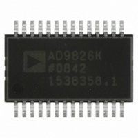
AD9826KRSZ Analog Devices Inc, AD9826KRSZ Datasheet

AD9826KRSZ
Specifications of AD9826KRSZ
Available stocks
Related parts for AD9826KRSZ
AD9826KRSZ Summary of contents
Page 1
AVDD AVSS VINR CDS VING CDS VINB CDS INPUT CLAMP OFFSET BIAS CDSCLK1 PRODUCT DESCRIPTION The AD9826 is a complete analog signal processor for imaging applications. It features a 3-channel architecture designed to sample and condition the outputs of ...
Page 2
AD9826–SPECIFICATIONS ANALOG SPECIFICATIONS Parameter MAXIMUM CONVERSION RATE 3-Channel Mode with CDS 2-Channel Mode with CDS 1-Channel Mode with CDS ACCURACY (ENTIRE SIGNAL PATH) ADC Resolution Integral Nonlinearity (INL) Differential Nonlinearity (DNL) No Missing Codes ANALOG INPUTS Input Signal Range (Programmable) ...
Page 3
DIGITAL SPECIFICATIONS Parameter LOGIC INPUTS High Level Input Voltage Low Level Input Voltage High Level Input Current Low Level Input Current Input Capacitance LOGIC OUTPUTS High Level Output Voltage Low Level Output Voltage High Level Output Current Low Level Output ...
Page 4
AD9826 ABSOLUTE MAXIMUM RATINGS With Respect Parameter To Min Max VIN, CAPT, CAPB AVSS –0.3 AVDD + 0.3 Digital Inputs AVSS –0.3 AVDD + 0.3 AVDD AVSS –0.5 +6.5 DRVDD DRVSS –0.5 +6.5 AVSS DRVSS –0.3 +0.3 Digital Outputs DRVSS ...
Page 5
Pin No. Mnemonic 1 CDSCLK1 2 CDSCLK2 3 ADCCLK 4 OEB 5 DRVDD 6 DRVSS SDATA 16 SCLK 17 SLOAD 18, 28 AVDD ...
Page 6
AD9826 DEFINITIONS OF SPECIFICATIONS INTEGRAL NONLINEARITY (INL) Integral nonlinearity error refers to the deviation of each individual code from a line drawn from “zero scale” through “positive full scale.” The point used as “zero scale” occurs 1/2 LSB before the ...
Page 7
GAIN SETTING Typical Performance Characteristics– 1.0 0.5 0 –0.5 –1.0 64000 200 0 ...
Page 8
AD9826 TIMING DIAGRAMS ANALOG t INPUTS CDSCLK1 t C1C2 CDSCLK2 t ADCLK ADCCLK t ADCLK OUTPUT DATA R(n–2) G(n–2) G(n–2) D<7:0> LOW HIGH BYTE BYTE It is recommended that CDSCLK falling edges do not occur within the ...
Page 9
ANALOG PIXEL INPUTS CDSCLK1 t t C1C2 C2 CDSCLK2 t C2ADR t ADC2 ADCCLK t ADCLK OUTPUT DATA CH1(n–2) D<7:0> HIGH LOW BYTE BYTE PIXEL n ANALOG INPUTS t C2 CDSCLK2 t C2ADR ...
Page 10
AD9826 ANALOG INPUTS CDSCLK2 t ADCLK ADCCLK t ADCLK OUTPUT R (n–2) G (n–2) G (n–2) DATA D<7:0> HIGH LOW BYTE BYTE ANALOG INPUTS CDSCLK2 ADCCLK t t ADCLK ADCLK OUTPUT DATA PIXEL (n–4) PIXEL (n–4) D<7:0> HIGH BYTE LOW ...
Page 11
ADCCLK t OD OUTPUT HIGH BYTE LOW BYTE DATA DB15–DB8 DB7–DB0 <D7:D0> PIXEL n PIXEL n OEB ADCCLK t OD OUTPUT HIGH BYTE DATA DB15–DB8 <D7:D0> PIXEL n OEB R/Wb SDATA SCLK t ...
Page 12
AD9826 ANALOG INPUTS CDSCLK1 CDSCLK2 ADCCLK RED RED (n–1) PGA OUT GREEN GREEN (n–1) PGA OUT BLUE PGA BLUE (n–1) OUT MUX GREEN (n–1) OUT OUTPUT DATA R(n–2) G(n–2) G(n–2) D<7:0> HIGH LOW BYTE BYTE NOTES 1. THE MUX STATE ...
Page 13
FUNCTIONAL DESCRIPTION The AD9826 can be operated in six different modes: 3-Channel CDS Mode, 3-Channel SHA Mode, 2-Channel CDS Mode, 2-Channel SHA Mode, 1-Channel CDS Mode, and 1-Channel SHA Mode. Each mode is selected by programming the Configura- tion Registers ...
Page 14
AD9826 adjust pin. A voltage applied to this pin will be subtracted from the voltages applied to the Red, Green, and Blue inputs in the first amplifier stage of the AD9826. The input clamp is disabled in this mode. For ...
Page 15
MUX Configuration Register The MUX Configuration Register controls the sampling chan- nel order and the 2-Channel Mode configuration in the AD9826. Bits D8 and D3–D0 should always be set low. Bit D7 is used when operating in 3-Channel or 2-Channel ...
Page 16
AD9826 CIRCUIT OPERATION Analog Inputs—CDS Mode Operation Figure 12 shows the analog input configuration for the CDS mode of operation. Figure 13 shows the internal timing for the sampling switches. The CCD reference level is sampled when CDSCLK1 transitions from ...
Page 17
SHA Mode Operation Analog Inputs— Figure 14 shows the analog input configuration for the SHA mode of operation. Figure 15 shows the internal timing for the sampling switches. The input signal is sampled when CDSCLK2 transitions from high to low, ...
Page 18
AD9826 Programmable Gain Amplifiers The AD9826 uses one Programmable Gain Amplifier (PGA) for each channel. Each PGA has a gain range from 1 (0 dB) to 6.0 (15.56 dB), adjustable in 64 steps. Figure 17 shows the PGA gain as ...
Page 19
Revision History Location Data Sheet changed from REV REV. A. Edits to ORDERING GUIDE . . . . . . . . . . . . . . . . ...
Page 20
...


