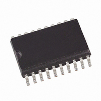
QT240-ISSG Atmel, QT240-ISSG Datasheet - Page 7

QT240-ISSG
Manufacturer Part Number
QT240-ISSG
Description
IC SENSOR QTOUCH 4CHAN 20SSOP
Manufacturer
Atmel
Series
Quantumr
Type
Signal Conditionerr
Datasheet
1.QT240-ISSG.pdf
(12 pages)
Specifications of QT240-ISSG
Input Type
Logic
Output Type
Logic
Current - Supply
1.5mA
Mounting Type
Surface Mount
Package / Case
20-SSOP
For Use With
427-1113 - BOARD EVAL FOR QT240-IS QTOUCH
Lead Free Status / RoHS Status
Lead free / RoHS Compliant
Interface
-
Other names
427-1102-2
QT240-ISS-G
QT240-ISS-G
Available stocks
Company
Part Number
Manufacturer
Quantity
Price
Part Number:
QT240-ISSG
Manufacturer:
ATMEL/爱特梅尔
Quantity:
20 000
3.2 Power Supply, PCB Layout
The power supply can range from 3.9 to 5. 5 volts. If this
fluctuates slowly with temperature, the device will track and
compensate for these changes automatically with only minor
changes in sensitivity. If the supply voltage drifts or shift s
quickly, the drift compensation mechanism will not be able to
keep up, causing sensitivity anomalies or false detections.
The QT240 will track slow changes in Vdd, but can be
seriously affected by rapid voltage steps.
If the supply is shared with another electronic system, care
should be taken to assure that the supply is free of digital
spikes, sags, and surges which can cause adverse effects.
The supply is best locally regulated using almost any
three-terminal LDO device from 4.0V to 5V.
For proper operation a 0.1µF or greater bypass capacitor
must be used between Vdd and Vss; the bypass capacitor
should be placed very close to the device Vss and Vdd pins.
The PCB should, if possible, include a copper pour under
and around the IC, but not extensively under the SNS lines.
3.3 Oscillator; Spread Spectrum
The oscillator is an internal type using an external current
bias source. Normal operation occurs at ~100 kHz ±20% with
R=62K at Vdd = 4.0V.
In Fast mode the oscillator can be spread-spectrum
modulated with a simple external RC network to avoid
dwelling on any one frequency. The circuit works by current
modulating the oscillator bias to provide a chirp modulation
within each burst. This helps dramatically with both RF
emissions and susceptibility. The circuit for this is shown in
Figure 1.2. The SYNC/SS pin outputs a rectangular pulse
with a period of one burst. At the end of the burst, SYNC/SS
clamps to ground. This forms a sawtooth modulation
waveform to create the frequency chirp modulation
(Figure 3.1).
The detection integrator (DI) filters out false detections
caused by interference on up to any six of these acquisitions.
The DI is a consensus filter that throws out a pending
detection if even one of the six samples does not confirm a
detection. As a result of this feature, it is extremely difficult
for an external signal to interfere with the device.
The typical modulation band of this circuit is ±7% around the
center frequency.
The oscillator frequency can be measured by
observing the acquisition pulses on any sense
channel with an oscilloscope. The first two
positive pulses in each burst will be exactly
10µs from rising edge to rising edge (100kHz) if
the oscillator is set correctly ( no spread
spectrum). Some subsequent pulse pairs will
have wider spacings; this is normal.
If desired the response time of the device in
Fast mode can be modified by altering the
oscillator frequency. The device can be set to
any center frequency from 20kHz to 150kHz by
simply altering the value of the bias resistor.
Lower values of R will speed up the device.
Higher resistor values will slow down the device
and reduce power consumption.
Slow mode relies on an internal RC timer which
cannot be adjusted via the bias resistor. During
intervals between bursts in Slow mode, the
100kHz oscillator is disabled.
lQ
7
Figure 3.1 Spread-spectrum Waveforms
Spread Spectrum in Slow Mode: The QT240 does not
support spread spectrum in Slow mode directly via the
SYNC/SS pin. However, the designer can still implement
spread spectrum by modulating the oscillator through a
resistor to OSC with a triangle or sawtooth wave.
The modulation signal should be exactly synchronous with
each burst, so that the resulting acquired signal is modulated
in the same way. If this rule is not followed, the signals will
contain modulation noise and false detections may occur.
3.4 Unused Channels
Unused SNS pins should not be left open. They should have
a small-value noncritical dummy Cs capacitor plus a 2.2K
series-R connected to their SNS pins to allow the internal
circuit to continue to function properly. A nominal value of
1nF (1,000pF) X7R ceramic will suffice.
Unused channels should not have sense traces or
electrodes connected to them except for the required option
resistors, which must always be installed and connected to
Vdd or Vss.
3.5 ESD Protection
Normally, only a series resistor is required for ESD
suppression. A 22K Rsns resistor in series with the sense
trace is sufficient in most cases. The dielectric panel (glass
or plastic) usually provides a high degree of isolation to
prevent ESD discharge from reaching the circuit . Rsns
should be placed close to the chip.
If the Cx load is high, Rsns can prevent total charge and
transfer and as a result gain can deteriorate. If a reduction in
Rsns increases gain noticeably, the lower value should be
used. Conversely, increasing the Rsns can result in added
ESD and EMC benefits provided that the increase does not
decrease sensitivity.
3.6 Crosstalk Precautions
Adjacent sense traces might require intervening ground
traces in order to reduce capacitive cross bleed if high
sensitivity is required or high values of delta-Cx are
anticipated (for example, from direct human touch to an
electrode connection). In normal touch applications behind
plastic panels this is almost never a problem regardless of
how the electrodes are wired.
QT240R R1.11/1006


