CC-2401K2A-CS Copeland Communications Inc, CC-2401K2A-CS Datasheet - Page 32
CC-2401K2A-CS
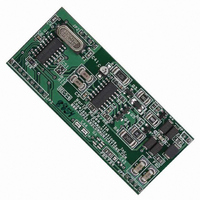
Manufacturer Part Number
CC-2401K2A-CS
Description
MODEM 2400BAUD SECURE 3.3V
Manufacturer
Copeland Communications Inc
Datasheet
1.CC-2401K2A-CS.pdf
(66 pages)
Specifications of CC-2401K2A-CS
Data Format
V.21, V.22, V.23, Bell 103
Baud Rates
2.4k
Interface
UART
Voltage - Supply
3 V ~ 3.6 V
Mounting Type
Surface Mount
Package / Case
Module
For Use With
539-1002 - KIT EVALUATION WORLD MODEM II
Lead Free Status / RoHS Status
Contains lead / RoHS non-compliant
Other names
539-1010
CC-2401K2A-CS
CC-2401K2A-CS


© 2007, Copeland Communications, Inc.
Register
*
NOTE: These registers are explained in detail in the following section.
SDB
SEC
SED
S3B
S3C
SDF
SE0
SE1
SE2
SE3
SE4
SE5
SE5
SE5
SE5
SE6
SE6
SE6
SE8
SEB
SEE
S37
S39
S3A
S62
S82
SF0
SF1
SF2
SF3
“S”
Register
Address
(hex)
0xDB
0xEC
0xED
0x3B
0x3C
0xDF
0xE0
0xE1
0xE2
0xE3
0xE4
0xE5
0xE5
0xE5
0xE5
0xE6
0xE6
0xE6
0xE8
0xEB
0xEE
0x37
0x39
0x3A
0x62
0x82
0xF0
0xF1
0xF2
0xF3
DSPR4
GPIO1
GPIO2
DGSR
DADH
Name
DADL
DSP1
DSP2
DSP3
CIDG
DAA0
DAA1
DAA2
DAA3
CRD
GPD
DDH
CDT
DDL
TPD
ATD
LVS
CF1
CF5
RV1
RV2
RV3
RC
IST
RP
S-Register Summary (Continued)
Function
Carrier detect return. Minimum length of time that a
carrier must return and be detected in order to be
recognized after a carrier loss is detected (5/3 ms units).
Carrier detect timeout. Amount of time modem waits for
carrier detect before aborting a call (1 second units).
Delay between going off hook and answer tone
generation when in answer mode (53.33 ms units).
Minimum number of consecutive ring pulses per ring
burst.
This is a bit-mapped register
This is a bit-mapped register
This is a bit-mapped register
Line Voltage Status. Eight bit signed 2’s complement
number representing the tip-ring voltage. Each bit
represents 1 volt. Polarity of the voltage is represented by
the MSB (sign bit). 0000_0000 = Measured voltage is <
3V.
This is a bit-mapped register
This is a bit-mapped register
This is a bit-mapped register
This is a bit-mapped register
This is a bit-mapped register
This is a bit-mapped register
(SE8 = 0x00) Write only definition. DSP register address
lower bits [7:0].
(SE8 = 0x01) Write only definition. DSP data word lower
bits [7:0].
(SE8 = 0x02) Read only definition. This is a bit-mapped
register
(SE8 = 0x02) Write only definition. This is a bit-mapped
register
(SE8 = 0x00) Write only definition. DSP register address
upper bits [15:8].
(SE8 = 0x01) Write only definition. DSP data word upper
bits [13:8].
(SE8 = 0x02) Write only definition. This is a bit-mapped
register
Set the mode to define E5 and E6 for low level DSP
control.
This is a bit-mapped register
This is a bit-mapped register
This is a bit-mapped register
This is a bit-mapped register
This is a bit-mapped register
This is a bit-mapped register
This is a bit-mapped register
Line current Status. 8 bit value returning the loop current.
Each bit represents 1.1 mA of loop current. Accuracy is
not guaranteed if the loop current is less than required for
normal operation
Page 32 of 66
Data Sheet
*
*
*
*
*
*
*
*
*
*
*
*
*
*
*
*
*
*
*
*
*
CC-2401K2 Datasheet Rev 1.5
CC-2401K2
Reset
0x3C
0x0C
0x0C
0x20
0x29
0x03
0x01
0x41
0x08
0x22
0x04
0x00
0x00
0x00
0x00
0x00
0x00
0x00
0x00
0x00
0x00
0x00
0x00
0x88
0x19
0x16
0x40
0x00
0x00
Related parts for CC-2401K2A-CS
Image
Part Number
Description
Manufacturer
Datasheet
Request
R

Part Number:
Description:
170 FOOT 24 CONDUCTOR, ST/ST, 100 MICRON, NUMBERED WITH PULLING EYE, INDIVIDUAL FIBERS ARE BUNDLED TOGETHER
Manufacturer:
DIGITHEAD
Part Number:
Description:
Relay; SSR; Cur-Rtg 25 A; Ctrl-V 4-32 VDC; Vol-Rtg 24-280 VAC; Panel; Key Locking Conn
Manufacturer:
Crydom Company
Datasheet:
Part Number:
Description:
Relay; SSR; Cur-Rtg 25 A; Ctrl-V 4-32 VDC; Vol-Rtg 24-280 VAC; Panel; Four Pin Screw
Manufacturer:
Crydom Company
Datasheet:
Part Number:
Description:
Relay; SSR; Cur-Rtg 50 A; Ctrl-V 4-32 VDC; Vol-Rtg 24-280 VAC; Panel; Four Pin Spring
Manufacturer:
Crydom Company
Datasheet:

Part Number:
Description:
CONV DC/DC 3W SNG 24V 3.3V PCB
Manufacturer:
TDK Corporation
Datasheet:
Part Number:
Description:
CONV DC/DC 6W SNGL 24V 12V PCB
Manufacturer:
TDK Corporation
Datasheet:
Part Number:
Description:
CONV DC/DC 6W SNGL 24V 5V PCB
Manufacturer:
TDK Corporation
Datasheet:
Part Number:
Description:
CONV DC/DC 6W SNGL 24V 3.3V PCB
Manufacturer:
TDK Corporation
Datasheet:
Part Number:
Description:
CONV DC/DC 10W SNGL 24V 5V PCB
Manufacturer:
TDK Corporation
Datasheet:

Part Number:
Description:
MODEM 2400BAUD SECURE 5V
Manufacturer:
Copeland Communications Inc
Datasheet:
Part Number:
Description:
MODEM 2400BAUD SERIAL 5V
Manufacturer:
Copeland Communications Inc
Datasheet:
Part Number:
Description:
MODEM 56KBAUD SERIAL V.92 5V
Manufacturer:
Copeland Communications Inc
Datasheet:

Part Number:
Description:
MODEM 2400 BAUD SERIAL
Manufacturer:
Copeland Communications Inc

Part Number:
Description:
MODEM 56K V.92 SERIAL
Manufacturer:
Copeland Communications Inc