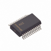
MAX7326AEG+ Maxim Integrated Products, MAX7326AEG+ Datasheet - Page 11

MAX7326AEG+
Manufacturer Part Number
MAX7326AEG+
Description
IC I/O EXPANDER I2C 16B 24QSOP
Manufacturer
Maxim Integrated Products
Datasheet
1.MAX7326ATG.pdf
(20 pages)
Specifications of MAX7326AEG+
Interface
I²C
Number Of I /o
16
Interrupt Output
Yes
Frequency - Clock
400kHz
Voltage - Supply
1.71 V ~ 5.5 V
Operating Temperature
-40°C ~ 125°C
Mounting Type
Surface Mount
Package / Case
24-QSOP
Includes
POR
Lead Free Status / RoHS Status
Lead free / RoHS Compliant
The acknowledge bit is a clocked 9th bit the recipient
uses to acknowledge receipt of each byte of data
(Figure 4). Each byte transferred effectively requires 9
bits. The master generates the 9th clock pulse, and the
recipient pulls down SDA during the acknowledge
clock pulse, so the SDA line is stable low during the
high period of the clock pulse. When the master is
transmitting to the MAX7326, the MAX7326 generates
the acknowledge bit because the device is the recipi-
ent. When the MAX7326 is transmitting to the master,
the master generates the acknowledge bit because the
master is the recipient.
The MAX7326 has two different 7-bit slave addresses
(Figure 5). The addresses are different to communicate
to the eight push-pull outputs, O8–O15, or the other
eight I/Os. The 8th bit following the 7-bit slave address
is the R/W bit. It is low for a write command and high for
a read command.
The first (A6), second (A5), and third (A4) bits of the
MAX7326 slave address are always 1, 1, and 0 (O0, O1,
Figure 4. Acknowledge
Figure 5. Slave Address
TRANSMITTER
SDA
RECEIVER
SCL
SDA BY
SDA BY
SCL
I
CONDITION
2
START
MSB
S
C Port Expander with 12 Push-Pull Outputs
1
______________________________________________________________________________________
1
A5
2
FOR ACKNOWLEDGMENT
A4
CLOCK PULSE
Slave Address
8
Acknowledge
A3
9
A2
I2–I5, O6, and O7) or 1, 0, and 1 (O8–O15). Connect
AD0 and AD2 to GND, V+ , SDA, or SCL to select slave
address bits A3, A2, A1, and A0. The MAX7326 has 16
possible slave addresses
to 16 MAX7326 devices on an I
The MAX7326 is accessed though an I
MAX7326 provides two different 7-bit slave addresses
for either the group A of eight ports (O0, O1, I2–I5, O6,
O7) or the group B of eight ports (O8–O15). See Tables
2 and 3.
A single-byte read from the group A ports of the
MAX7326 returns the status of the four input ports and
four output ports (read back as inputs), and clears both
the internal transition flags and the INT output when the
master acknowledges the salve address byte. A single-
byte read from the group B ports of the MAX7326
returns the status of the eight output ports, read back
as inputs.
A 2-byte read from the group A ports of the MAX7326
returns the status of the four input ports (as for a single-
byte read), followed by the four transition flags for the
four input ports and four output ports. The internal tran-
sition flags and the INT output are cleared when the
master acknowledges the slave address byte, but the
previous transition flag data is sent as the second byte.
A 2-byte read from the group B ports of the MAX7326
repeatedly returns the status of the eight output ports,
read back as inputs.
A multibyte read (more than 2 bytes before the I
STOP bit) from the group A ports of the MAX7326
repeatedly returns the port data, followed by the transi-
tion flags. As the data is resampled for each transmis-
sion, and the transition flags are reset each time, a
multibyte read continuously returns the current data
and identifies any changing input ports.
A1
LSB
A0
and 4 Inputs
(Tables
Accessing the MAX7326
2
C bus.
R/W
2 and 3), allowing up
2
C interface. The
ACK
2
11
C


