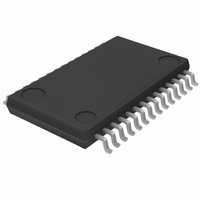
BU9929FV Rohm Semiconductor, BU9929FV Datasheet - Page 9

BU9929FV
Manufacturer Part Number
BU9929FV
Description
IC I/O EXPANDER I2C 16B 28SSOP
Manufacturer
Rohm Semiconductor
Datasheet
1.BU9929FV.pdf
(12 pages)
Specifications of BU9929FV
Interface
I²C
Number Of I /o
16
Interrupt Output
Yes
Frequency - Clock
400kHz
Voltage - Supply
3 V ~ 5.5 V
Operating Temperature
-15°C ~ 75°C
Mounting Type
Surface Mount
Package / Case
28-SSOP
Lead Free Status / RoHS Status
Lead free / RoHS Compliant
Available stocks
Company
Part Number
Manufacturer
Quantity
Price
Company:
Part Number:
BU9929FV-E2
Manufacturer:
CY
Quantity:
18
Part Number:
BU9929FV-E2
Manufacturer:
ROHM/罗姆
Quantity:
20 000
Multimedia ICs
3.Condition change detection result output mode
1) This IC becomes I
2Byte Watching
1Byte Watching
<DATA Keeping Operation>
In a case that there is a change in detection port during detection result transmission, then watching data is saved by the
end of detection output, and it will be proceeded further after the detection output is finished.
However, the output data in this case will be “AND” output of every bits of the watching data.
2) DS pin Description
By DS pin, valid/invalid of condition detection of the default condition (from RESET release to reception of the first I
command) can be set.
<DS pic valid range>
In the range from RESET release to the first set of condition detection mode by I
valid. After the set of condition detection mode by I
will be reflected.
<Pin setting>
DS pin= “H” : Input bit condition detection mode is valid.
But, 1 byte detection mode (only PION7-PION0 will be in condition detection)
DS pin=“L” : Input bit condition detection mode is invalid.
St
St
Watching Ports
Output for I
0 0 0 1 0 0 0
0 0 0 1 0 0 0
2
C BUS
2
C master device, and the detection result is sent according to the following format;
W
W
A
A
SLAVE ADDRESS +0
SLAVE ADDRESS +0
FE
In the case of Arbitration;
Output is delayed
FE
2
C command, this pin will be invalid, and the set by I
A
A
PION7 − PION0
WRITE DATA 1
PION7 − PION0
WRITE DATA 1
FC
FC
F0
A
A
2
Sp
C command, the set of this pin will be
WRITE DATA 2
PIO15 − PIO8
F8
AND Output of every bits of
the watching data
F0
BU9929FV
A Sp
2
C commanded
9/11
2
C


