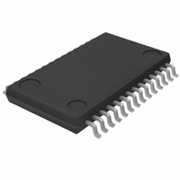
BU9929FV Rohm Semiconductor, BU9929FV Datasheet

BU9929FV
Specifications of BU9929FV
Available stocks
Related parts for BU9929FV
BU9929FV Summary of contents
Page 1
... Recommended operating conditions (Ta=25°C) Parameter Min. Operating supply voltage range 3 BUS interface. It also contains monitoring function that conveys 2 C BUS BUS master function Limits Unit 7.0 V 640 mW −15 to +75 ˚C −55 to +125 ˚C GND−0 +0 Typ. Max. Unit − 5.5 V BU9929FV 2 C BUS. 1/11 ...
Page 2
... TEST0 PION0 5 PION1 6 PION2 7 8 PION3 PION4 9 PION5 10 PION6 11 INT 12 PION7 13 GND 14 TIMING CONTROLLER DATA LATCH BLOCK SLAVE ADDRESS 2 BITS PIO BUFFER BU9929FV DEFAULT STATUS DS EDGE DETECT INT BLOCK CLK RESB 26 25 PIO15 PIO14 24 23 PIO13 PIO12 22 21 PIO11 20 PIO10 19 PIO9 ...
Page 3
... This waits for condition detection function of input. Output will be Hi-Z at Shut Down mode. 5V input is possible when this IC is operated by 3.3V. Standard input/output terminal. Input at TTL level. This waits for condition detection function of input. Output will be Hi-Z at Shut Down mode. GND terminal BU9929FV Pin Description 3/11 ...
Page 4
... At Shut Down mode, clock supply into this IC will be shut down. Power terminal. 3.3V/5.0V should be put in. Input terminal for setting of I Slave address lower 2 bits. IC TEST Pin. "L" Input required for normal operation. IC TEST Pin. "L" Input required for normal operation. BU9929FV Pin Description 2 C BUS 4/11 ...
Page 5
... 0.0 0.2 0 0.0 0.2 0 − 100 250 ns CL=400pF BU9929FV Conditions Test Pin No 15-17 3-5, 11, 13 15-27 5-11, 13 3-5, 11, 13 15-27 3-5, 11, 13 15-27 18-25 =4mA 5-13, 18-25 =4mA 1, 2 =6mA =6mA 1, 2 5/11 ...
Page 6
... Timing) SCL SDA (Data Timing) SCL SDA DAT (Stop Timing) SCL SDA =5.0V, Ta=25° LSB Min. Max. Unit f SCL 0 400 kHz − µs 0.6 − µs 0.6 − 100 ns µs 0 0.9 − µs 0 STA STA DAT STO BU9929FV 6/11 ...
Page 7
... D2 : Watching object input choice 0 : PION0 to PION7 1 : PION8 to PIO15 D1 : Change detection mode 0 : Falling edge 1 : Both rising and falling edge D0 : Input port condition watching mode 0 : Invalid 1 : Valid WRITE DATA 1 A PION7 − PION0 PIO15 − PIO8 DIR ON BYTE SEL EDGE SEL BU9929FV WRITE DATA DET ON 7/11 ...
Page 8
... IC PAD Input Schmitt Input Port sampling timing As shown below, BU9929FV is sampling for Input Ports with the rising edges of CLK. Therefore it is necessary that Input Ports are keeping at least 1 CLK cycle, for their certain inputs. Watching Ports CLK A READ DATA 2 PION7 − ...
Page 9
... A WRITE DATA 1 PION7 − PION0 A WRITE DATA 1 PION7 − PION0 the case of Arbitration; Output is delayed command, this pin will be invalid, and the set by I BU9929FV A WRITE DATA PIO15 − PIO8 AND Output of every bits of the watching data command, the set of this pin will be ...
Page 10
... Watching Ports F6 2 Output for I C BUS CLK INT OUTPUT St SLAVE ADDRESS C7 A4 " A term" St SLAVE ADDRESS BU9929FV 2 C Data A OUTPUT "F8" OUTPUT "84" OUTPUT "84hex data" which is the result of AND data for "F6", "C7" and " A4". 10/11 ...
Page 11
... Contents of each register before shut down will be saved by the shut down release External dimensions (Unit : mm) 10.0±0 0.65 0.22±0.1 0.3Min. SSOP-B28 AA St SLAVE ADDRESS 0.1 BU9929FV R A OUTPUT "AA" Data "78h" is not kept, the output data is immediately before sampled data. 11/11 ...
Page 12
Appendix No technical content pages of this document may be reproduced in any form or transmitted by any means without prior permission of ROHM CO.,LTD. The contents described herein are subject to change without notice. The specifications for the product ...


