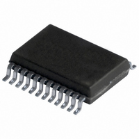
PCF8575TS/1,118 NXP Semiconductors, PCF8575TS/1,118 Datasheet - Page 8

PCF8575TS/1,118
Manufacturer Part Number
PCF8575TS/1,118
Description
IC I/O EXPANDER I2C 16B 24SSOP
Manufacturer
NXP Semiconductors
Datasheet
1.PCF8575TS1112.pdf
(24 pages)
Specifications of PCF8575TS/1,118
Package / Case
24-SSOP
Interface
I²C
Number Of I /o
16
Interrupt Output
Yes
Frequency - Clock
400kHz
Voltage - Supply
4.5 V ~ 5.5 V
Operating Temperature
-40°C ~ 85°C
Mounting Type
Surface Mount
Includes
POR
Logic Family
PCF8575
Operating Supply Voltage
2.5 V to 5.5 V
Power Dissipation
400 mW
Operating Temperature Range
- 40 C to + 85 C
Logic Type
I/O Expander
Maximum Clock Frequency
400 KHz
Mounting Style
SMD/SMT
Output Current
25 mA
Lead Free Status / RoHS Status
Lead free / RoHS Compliant
Lead Free Status / RoHS Status
Lead free / RoHS Compliant, Lead free / RoHS Compliant
Other names
568-1079-2
935276552118
PCF8575TSDB-T
935276552118
PCF8575TSDB-T
Available stocks
Company
Part Number
Manufacturer
Quantity
Price
Company:
Part Number:
PCF8575TS/1,118
Manufacturer:
Skyworks
Quantity:
1 714
dbook, full pagewidth
Philips Semiconductors
7
7.1
The PCF8575’s 16 ports (see Fig.7) are entirely independent and can be used either as input or output ports. Input data
is transferred from the ports to the microcontroller in the READ mode (see Fig.10). Output data is transmitted to the ports
in the WRITE mode (see Fig.9).
This quasi-bidirectional I/O can be used as an input or output without the use of a control signal for data direction.
At power-on the I/Os are HIGH. In this mode only a current source (I
V
and are switched off by the negative edge of SCL. The I/Os should be HIGH before being used as inputs. After power-on
as all the I/Os are set HIGH all of them can be used as input. Any change in setting of the I/Os as either inputs or outputs
can be done with the write mode. Warning: If a HIGH is applied to an I/O which has been written earlier to LOW, a large
current (I
7.2
Figures 8, 9 and 10 show the address and timing diagrams. Before any data is transmitted or received the master must
send the address of the receiver via the SDA line. The first byte transmitted after the START condition carries the address
of the slave device and the read/write bit. The address of the slave device must not be changed between the START and
the STOP conditions. The PCF8575 acts as a slave receiver or a slave transmitter.
1999 Apr 07
DD
Remote 16-bit I/O expander for I
FUNCTIONAL DESCRIPTION
(I
OHt
Quasi-bidirectional I/Os
Addressing
) allows fast rising edges into heavily loaded outputs. These devices turn on when an output is written HIGH,
OL
) will flow to V
write pulse
data from
shift register
power-on
reset
read pulse
data to
shift register
SS
. (see Characteristics note 3).
Fig.8 Byte containing the slave address and the R/W bits.
handbook, halfpage
Fig.7 Simplified schematic diagram of each I/O.
C I
D
FF
S
Q
S
0
1
C I
D
2
FF
S
slave address
C-bus
0
Q
0
I OHt
8
A2
A1
OH
100
A0 R/W
A
) to V
I OH
I OL
MGL541
DD
A
is active. An additional strong pull-up to
MGL540
V DD
V SS
P00 to P07
P10 to 17
to interrupt
logic
Product specification
PCF8575


