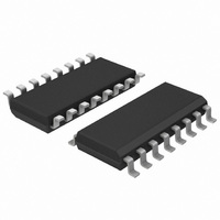
PCA9557D/DG,118 NXP Semiconductors, PCA9557D/DG,118 Datasheet - Page 6

PCA9557D/DG,118
Manufacturer Part Number
PCA9557D/DG,118
Description
IC I/O PORT I2C/SMBUS 16-SOIC
Manufacturer
NXP Semiconductors
Datasheet
1.PCA9557BS118.pdf
(26 pages)
Specifications of PCA9557D/DG,118
Interface
I²C, SMBus
Number Of I /o
8
Interrupt Output
No
Frequency - Clock
400kHz
Voltage - Supply
2.3 V ~ 5.5 V
Operating Temperature
-40°C ~ 85°C
Mounting Type
Surface Mount
Package / Case
16-SOIC (3.9mm Width)
Includes
POR
Lead Free Status / RoHS Status
Lead free / RoHS Compliant
Other names
935285892118
NXP Semiconductors
6. System diagram
PCA9557
Product data sheet
Fig 7.
RESET
SDA
SCL
A2
A1
A0
System diagram
or
or
or
1.1 k
1.6 k
1.6 k
1.1 k
1.1 k
1.1 k
Table 3.
[1]
Symbol
V
IO2
IO3
IO4
IO5
IO6
IO7
RESET
V
SS
DD
HVQFN16 package die supply ground is connected to both the V
V
electrical, and board-level performance, the exposed pad needs to be soldered to the board using a
corresponding thermal pad on the board, and for proper heat conduction through the board thermal vias
need to be incorporated in the PCB in the thermal pad region.
SS
I
2
C-BUS/SMBus
INTERFACE
pin must be connected to the supply ground for proper device operation. For enhanced thermal,
LOGIC
Pin description
Pin
SO16, TSSOP16
8
9
10
11
12
13
14
15
16
Rev. 06 — 11 June 2008
INPUT
PORT
…continued
Q7
Q6
Q5
Q4
Q3
Q2
Q1
Q0
INVERSION
POLARITY
HVQFN16
6
7
8
9
10
11
12
13
14
[1]
Q7
Q6
Q5
Q4
Q3
Q2
Q1
Q0
8-bit I
Description
supply ground
input/output 2
input/output 3
input/output 4
input/output 5
input/output 6
input/output 7
active LOW reset input
supply voltage
CONFIG.
2
C-bus and SMBus I/O port with reset
Q7
Q6
Q5
Q4
Q3
Q2
Q1
Q0
SS
pin and the exposed center pad. The
OUTPUT
PORT
Q7
Q6
Q5
Q4
Q3
Q2
Q1
Q0
PCA9557
© NXP B.V. 2008. All rights reserved.
002aad276
1.1 k
IO0
IO1
IO2
IO3
IO4
IO5
IO6
IO7
6 of 26


