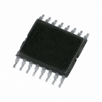
PCA9534PW,118 NXP Semiconductors, PCA9534PW,118 Datasheet - Page 13

PCA9534PW,118
Manufacturer Part Number
PCA9534PW,118
Description
IC I/O EXPANDER I2C 8B 16TSSOP
Manufacturer
NXP Semiconductors
Datasheet
1.PCA9534BS118.pdf
(25 pages)
Specifications of PCA9534PW,118
Package / Case
16-TSSOP
Interface
I²C, SMBus
Number Of I /o
8
Interrupt Output
Yes
Frequency - Clock
400kHz
Voltage - Supply
2.3 V ~ 5.5 V
Operating Temperature
-40°C ~ 85°C
Mounting Type
Surface Mount
Includes
POR
Logic Family
PCA9534
Number Of Lines (input / Output)
8.0 / 8.0
Operating Supply Voltage
2.3 V to 5.5 V
Power Dissipation
200 mW
Operating Temperature Range
- 40 C to + 85 C
Input Voltage
5 V
Logic Type
I2C, SMBus
Maximum Clock Frequency
400 KHz
Mounting Style
SMD/SMT
Number Of Input Lines
8.0
Number Of Output Lines
8.0
Output Current
50 mA
Output Voltage
5 V
Lead Free Status / RoHS Status
Lead free / RoHS Compliant
Lead Free Status / RoHS Status
Lead free / RoHS Compliant, Lead free / RoHS Compliant
Other names
568-1834-2
935275051118
PCA9534PW-T
935275051118
PCA9534PW-T
Available stocks
Company
Part Number
Manufacturer
Quantity
Price
Part Number:
PCA9534PW,118
Manufacturer:
NXP/恩智浦
Quantity:
20 000
NXP Semiconductors
[1]
[2]
[3]
10. Dynamic characteristics
Table 10.
[1]
[2]
[3]
PCA9534_3
Product data sheet
Symbol
f
t
t
t
t
t
t
t
t
t
t
t
t
t
Port timing
t
t
t
Interrupt timing
t
t
SCL
BUF
HD;STA
SU;STA
SU;STO
HD;DAT
VD:ACK
VD;DAT
SU;DAT
LOW
HIGH
r
f
SP
v(Q)
su(D)
h(D)
v(INT_N)
rst(INT_N)
V
Each I/O must be externally limited to a maximum of 25 mA and the device must be limited to a maximum current of 100 mA.
The total current sourced by all I/Os must be limited to 85 mA.
t
t
C
VD;ACK
VD;DAT
DD
b
= total capacitance of one bus line in pF.
must be lowered to 0.2 V in order to reset part.
= minimum time for SDA data output to be valid following SCL LOW.
= time for Acknowledgement signal from SCL LOW to SDA (out) LOW.
Dynamic characteristics
Parameter
SCL clock frequency
bus free time between a STOP and
START condition
hold time (repeated) START condition
set-up time for a repeated START
condition
set-up time for STOP condition
data hold time
data valid acknowledge time
data valid time
data set-up time
LOW period of the SCL clock
HIGH period of the SCL clock
rise time of both SDA and SCL signals
fall time of both SDA and SCL signals
pulse width of spikes that must be
suppressed by the input filter
data output valid time
data input setup time
data input hold time
valid time on pin INT
reset time on pin INT
Rev. 03 — 6 November 2006
Conditions
8-bit I
2
C-bus and SMBus low power I/O port with interrupt
[1]
[2]
Standard-mode
Min
300
250
100
4.7
4.0
4.7
4.0
0.3
4.7
4.0
0
0
1
-
-
-
-
-
-
I
2
C-bus
1000
Max
3.45
100
300
200
50
4
4
-
-
-
-
-
-
-
-
-
-
-
20 + 0.1C
20 + 0.1C
Fast-mode I
Min
100
100
1.3
0.6
0.6
0.6
0.1
1.3
0.6
50
0
0
1
-
-
-
-
PCA9534
b
b
© NXP B.V. 2006. All rights reserved.
[3]
[3]
2
C-bus
Max
400
300
300
200
0.9
50
4
4
-
-
-
-
-
-
-
-
-
-
-
13 of 25
Unit
kHz
ns
ns
ns
ns
ns
ns
s
s
s
s
s
s
s
s
s
s
s
s


