PCA9555N,112 NXP Semiconductors, PCA9555N,112 Datasheet - Page 5
PCA9555N,112
Manufacturer Part Number
PCA9555N,112
Description
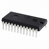
IC I/O EXPANDER I2C 16B 24DIP
Manufacturer
NXP Semiconductors
Datasheet
1.PCA9555BS118.pdf
(34 pages)
Specifications of PCA9555N,112
Package / Case
24-DIP (0.600", 15.24mm)
Interface
I²C, SMBus
Number Of I /o
16
Interrupt Output
Yes
Frequency - Clock
400kHz
Voltage - Supply
2.3 V ~ 5.5 V
Operating Temperature
-40°C ~ 85°C
Mounting Type
Through Hole
Includes
POR
Logic Family
PCA
Number Of Lines (input / Output)
16 / 16
Operating Supply Voltage
2.3 V to 5.5 V
Operating Temperature Range
- 40 C to + 85 C
Input Voltage
2.3 V to 5.5 V
Maximum Clock Frequency
400 KHz
Mounting Style
Through Hole
Number Of Input Lines
16
Number Of Output Lines
16
Lead Free Status / RoHS Status
Lead free / RoHS Compliant
For Use With
OM6285 - EVAL BOARD I2C-2002-1A568-4002 - DEMO BOARD I2C
Lead Free Status / Rohs Status
Lead free / RoHS Compliant
Other names
568-2027-5
935276768112
PCA9555N
935276768112
PCA9555N
Available stocks
Company
Part Number
Manufacturer
Quantity
Price
Company:

Part Number:
PCA9555N,112
Manufacturer:
SANREX
Quantity:
43


NXP Semiconductors
PCA9555_8
Product data sheet
5.2 Pin description
Table 3.
[1]
Symbol
INT
A1
A2
IO0_0
IO0_1
IO0_2
IO0_3
IO0_4
IO0_5
IO0_6
IO0_7
V
IO1_0
IO1_1
IO1_2
IO1_3
IO1_4
IO1_5
IO1_6
IO1_7
A0
SCL
SDA
V
SS
DD
HVQFN and HWQFN package die supply ground is connected to both the V
pad. The V
electrical, and board-level performance, the exposed pad needs to be soldered to the board using a
corresponding thermal pad on the board, and for proper heat conduction through the board thermal vias
need to be incorporated in the PCB in the thermal pad region.
Pin description
Pin
DIP24, SO24,
SSOP24, TSSOP24
1
2
3
4
5
6
7
8
9
10
11
12
13
14
15
16
17
18
19
20
21
22
23
24
SS
pin must be connected to supply ground for proper device operation. For enhanced thermal,
Rev. 08 — 22 October 2009
HVQFN24,
HWQFN24
22
23
24
1
2
3
4
5
6
7
8
9
10
11
12
13
14
15
16
17
18
19
20
21
[1]
16-bit I
2
Description
interrupt output (open-drain)
address input 1
address input 2
port 0 input/output
supply ground
port 1 input/output
address input 0
serial clock line
serial data line
supply voltage
C-bus and SMBus I/O port with interrupt
SS
pin and the exposed center
PCA9555
© NXP B.V. 2009. All rights reserved.
5 of 34
Related parts for PCA9555N,112
Image
Part Number
Description
Manufacturer
Datasheet
Request
R

Part Number:
Description:
Manufacturer:
NXP Semiconductors
Datasheet:
Part Number:
Description:
NXP Semiconductors designed the LPC2420/2460 microcontroller around a 16-bit/32-bitARM7TDMI-S CPU core with real-time debug interfaces that include both JTAG andembedded trace
Manufacturer:
NXP Semiconductors
Datasheet:

Part Number:
Description:
NXP Semiconductors designed the LPC2458 microcontroller around a 16-bit/32-bitARM7TDMI-S CPU core with real-time debug interfaces that include both JTAG andembedded trace
Manufacturer:
NXP Semiconductors
Datasheet:
Part Number:
Description:
NXP Semiconductors designed the LPC2468 microcontroller around a 16-bit/32-bitARM7TDMI-S CPU core with real-time debug interfaces that include both JTAG andembedded trace
Manufacturer:
NXP Semiconductors
Datasheet:
Part Number:
Description:
NXP Semiconductors designed the LPC2470 microcontroller, powered by theARM7TDMI-S core, to be a highly integrated microcontroller for a wide range ofapplications that require advanced communications and high quality graphic displays
Manufacturer:
NXP Semiconductors
Datasheet:
Part Number:
Description:
NXP Semiconductors designed the LPC2478 microcontroller, powered by theARM7TDMI-S core, to be a highly integrated microcontroller for a wide range ofapplications that require advanced communications and high quality graphic displays
Manufacturer:
NXP Semiconductors
Datasheet:
Part Number:
Description:
The Philips Semiconductors XA (eXtended Architecture) family of 16-bit single-chip microcontrollers is powerful enough to easily handle the requirements of high performance embedded applications, yet inexpensive enough to compete in the market for hi
Manufacturer:
NXP Semiconductors
Datasheet:
Part Number:
Description:
The XA-S3 device is a member of Philips Semiconductors? XA(eXtended Architecture) family of high performance 16-bitsingle-chip microcontrollers
Manufacturer:
NXP Semiconductors
Datasheet:

Part Number:
Description:
The NXP BlueStreak LH75401/LH75411 family consists of two low-cost 16/32-bit System-on-Chip (SoC) devices
Manufacturer:
NXP Semiconductors
Datasheet:
Part Number:
Description:
The NXP LPC3130/3131 combine an 180 MHz ARM926EJ-S CPU core, high-speed USB2
Manufacturer:
NXP Semiconductors
Datasheet:
Part Number:
Description:
The NXP LPC3141 combine a 270 MHz ARM926EJ-S CPU core, High-speed USB 2
Manufacturer:
NXP Semiconductors
Part Number:
Description:
The NXP LPC3143 combine a 270 MHz ARM926EJ-S CPU core, High-speed USB 2
Manufacturer:
NXP Semiconductors

Part Number:
Description:
The NXP LPC3152 combines an 180 MHz ARM926EJ-S CPU core, High-speed USB 2
Manufacturer:
NXP Semiconductors
Part Number:
Description:
The NXP LPC3154 combines an 180 MHz ARM926EJ-S CPU core, High-speed USB 2
Manufacturer:
NXP Semiconductors