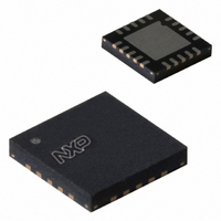
PCA9501BS,118 NXP Semiconductors, PCA9501BS,118 Datasheet - Page 7

PCA9501BS,118
Manufacturer Part Number
PCA9501BS,118
Description
IC I/O EXPANDER I2C 8B 20HVQFN
Manufacturer
NXP Semiconductors
Datasheet
1.PCA9501BS118.pdf
(28 pages)
Specifications of PCA9501BS,118
Package / Case
20-VQFN Exposed Pad, 20-HVQFN, 20-SQFN, 20-DHVQFN
Interface
I²C, SMBus
Number Of I /o
8
Interrupt Output
Yes
Frequency - Clock
400kHz
Voltage - Supply
2.5 V ~ 3.6 V
Operating Temperature
-40°C ~ 85°C
Mounting Type
Surface Mount
Includes
EEPROM
Logic Family
PCA9501
Number Of Lines (input / Output)
8.0 / 8.0
Operating Supply Voltage
2.5 V to 3.6 V
Power Dissipation
400 mW
Operating Temperature Range
- 40 C to + 85 C
Input Voltage
5 V
Logic Type
I/O Expander
Maximum Clock Frequency
400 KHz
Mounting Style
SMD/SMT
Number Of Input Lines
8.0
Number Of Output Lines
8.0
Output Current
25 mA
Output Voltage
5 V
Lead Free Status / RoHS Status
Lead free / RoHS Compliant
For Use With
OM6285 - EVAL BOARD I2C-2002-1A568-4002 - DEMO BOARD I2C
Lead Free Status / Rohs Status
Lead free / RoHS Compliant
Other names
568-3352-2
935273813118
PCA9501BS-T
935273813118
PCA9501BS-T
Available stocks
Company
Part Number
Manufacturer
Quantity
Price
Company:
Part Number:
PCA9501BS,118
Manufacturer:
Maxim
Quantity:
10
NXP Semiconductors
PCA9501_4
Product data sheet
Fig 9.
Transient pull-up current (I
SDA
IO3 output voltage
IO3 pull-up output current
SCL
7.3.1 Quasi-bidirectional I/Os
S
7.3.2 Interrupt
START condition
slave address (I/O expander)
1
0
A5 A4 A3 A2 A1 A0
2
A quasi-bidirectional I/O can be used as an input or output without the use of a control
signal for data direction. At power-on the I/Os are HIGH. In this mode, only a current
source to V
heavily loaded outputs. These devices turn on when an output is written HIGH, and are
switched off by the negative edge of SCL. The I/Os should be HIGH before being used as
inputs. See
The PCA9501 provides an open-drain output (INT) which can be fed to a corresponding
input of the microcontroller. This gives these chips a type of master function which can
initiate an action elsewhere in the system. See
An interrupt is generated by any rising or falling edge of the port inputs in the input mode.
After time t
Resetting and reactivating the interrupt circuit is achieved when data on the port is
changed to the original setting or data is read from or written to the port which has
generated the interrupt.
Resetting occurs as follows:
Each change of the I/Os after resetting will be detected and, after the next rising clock
edge, will be transmitted as INT. Reading from or writing to another device does not affect
the interrupt circuit.
3
•
•
•
•
4
In the Read mode at the acknowledge bit after the rising edge of the SCL signal
In the Write mode at the acknowledge bit after the HIGH-to-LOW transition of the SCL
signal
Returning of the port data to its original setting
Interrupts which occur during the acknowledge clock pulse may be lost (or very short)
due to the resetting of the interrupt during this pulse.
5
6
v(INT)
DD
Figure
7
OHt
R/W
is active. An additional strong pull-up to V
8
0
) while IO3 changes from LOW to HIGH and back to LOW
the signal INT is valid. See
9
A
acknowledge
from slave
9.
Rev. 04 — 10 February 2009
8-bit I
2
data to port
C-bus and SMBus I/O port with interrupt, 2-kbit EEPROM
IO3
1
I
OHt
Figure
A
acknowledge
from slave
Figure
11.
data to port
10.
DD
IO3
0
allows fast rising edges into
I
PCA9501
A
OH
acknowledge
from slave
© NXP B.V. 2009. All rights reserved.
002aad292
P
STOP
condition
7 of 28


