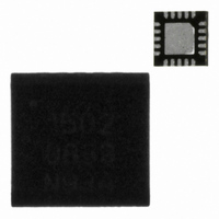
SX1502I087TRT Semtech, SX1502I087TRT Datasheet - Page 9

SX1502I087TRT
Manufacturer Part Number
SX1502I087TRT
Description
IC GPIO EXPANDER I2C 8CH 20QFN
Manufacturer
Semtech
Datasheet
1.SX1501I087TRT.pdf
(34 pages)
Specifications of SX1502I087TRT
Interface
I²C
Number Of I /o
8
Interrupt Output
Yes
Frequency - Clock
400kHz
Voltage - Supply
1.2 V ~ 5.5 V
Operating Temperature
-40°C ~ 85°C
Mounting Type
Surface Mount
Package / Case
20-QFN
Lead Free Status / RoHS Status
Lead free / RoHS Compliant
Other names
SX1502I087TR
Available stocks
Company
Part Number
Manufacturer
Quantity
Price
Company:
Part Number:
SX1502I087TRT
Manufacturer:
LTC
Quantity:
196
Part Number:
SX1502I087TRT
Manufacturer:
SEMTECH/美国升特
Quantity:
20 000
ADVANCED COMMUNICATIONS & SENSING
(1) Assuming no load connected to outputs and inputs fixed to VCC1,2 or GND.
(2) Can be increased in RegAdvanced register. Please refer to §2.2.1 for more details.
(3) All values referred to VIH
(4) A device must internally provide a hold time of at least 300ns for the SDA signal (referred to VIH
the falling edge of SCL.
(5) The maximum t
(6) A Fast-mode I
This will automatically be the case if the device does not stretch the LOW period of the SCL signal.
If such a device does stretch the LOW period of the SCL signal, it must output the next data bit to the SDA line t
= 1250 ns (according to the Standard-mode I2C-bus specification) before the SCL line is released.
(7) C
2.2.1
When bit 1 of RegAdvanced register is set, max IOH and IOL spec when VCC1,2 is below VBOOST can be
increased together with IDDM and ICC1,2 figures as described below.
Supply
I/Os set as Output
NINT, NRESET
Important: RegAdvanced register doesn’t affect any spec when VCC1 and VCC2 are above VBOOST.
Rev 9 – 5
Symbol
Miscellaneous
Symbol
VBOOST Low voltage boost threshold
RPULL
t
SU;STO
IDDM
t
t
V
ICC1
ICC2
V
IOL
BUF
C
b
PLD
IOH
IOL
t
nH
nL
= total capacitance of one bus line in pF. If mixed with Hs-mode devices, faster fall-times are allowed.
f
b
M
Increasing I/O Sink and Source Current Capabilities (Boost Mode)
th
August 2010
Description
Fall time of both SDA and
SCL signals
Set-up time for STOP
condition
Bus free time between a
STOP and START condition
Capacitive load for each bus
line
Noise margin at the LOW
level for each connected
device (including hysteresis)
Noise margin at the HIGH
level for each connected
device (including hysteresis)
Programmable pull-up/down
resistors for IO[0-7]
PLD propagation delay
Description
Main supply current
(I
I/O bank A supply current
I/O bank B supply current
High level output source
current for all I/Os
Low level output sink current
for the high sink I/Os
Low level output sink current
for the other I/Os
Low level output sink current
for NINT, NRESET
2
2
C inactive)
C-bus device can be used in a Standard-mode I
HD;DAT
has only to be met if the device does not stretch the LOW period (t
MR min
and VIL
Table 6 – Electrical Specifications in Boost Mode
M max
levels.
Table 5 – Electrical Specifications
VDDM = 5.5V (VCC1,2 < VBOOST)
VDDM = 1.2V (VCC1,2 < VBOOST)
VCC1,2 & VDDM = 1.2V
VCC1,2 & VDDM = 5V
SX1501/2
SX1503
SX1502
SX1503
Conditions
2
VCC1,2 >= VBOOST
VCC1,2 >= VBOOST
VCC1,2 >= VBOOST
C-bus system, but the requirement t
VDDM >= VBOOST
VCC1,2 < VBOOST
VCC1,2 < VBOOST
VCC1,2 < VBOOST
VDDM < VBOOST
9
-
-
-
-
-
-
-
Conditions
4/8/16 Channel Low Voltage GPIO
VCC1 = VBOOST
VCC1 = VBOOST
VCC2 = VBOOST
VCC2 = VBOOST
-
VCC1 = 1.2V
VCC1 = 1.2V
VCC2 = 1.2V
VCC2 = 1.2V
20+0.1C
LOW
0.1*VDDM
0.2*VDDM
SX1501/SX1502/SX1503
) of the SCL signal.
Min
0.6
1.3
-
-
-
-
MR min
b
(7)
SU;DAT
) to bridge the undefined region of
Min
2.0
-
-
-
-
-
-
-
-
-
-
-
-
-
-
-
-
-
-
Typ
60
250 ns must then be met.
r max
-
-
-
-
-
-
-
-
+ t
www.semtech.com
Typ
150
250
100
250
100
150
250
100
2.2
25
50
-
-
-
-
-
-
-
-
SU;DAT
Max
300
400
500
= 1000 + 250
25
Max Unit
-
-
-
-
-
250
350
200
400
200
250
150
450
200
2.4
50
24
12
12
12
8
4
6
6
Unit
mA
mA
mA
mA
k
µA
uA
µA
µA
µs
µs
pF
ns
ns
V
V
V


