PCA9535D,112 NXP Semiconductors, PCA9535D,112 Datasheet - Page 8
PCA9535D,112
Manufacturer Part Number
PCA9535D,112
Description
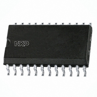
IC I/O EXPANDER I2C 16B 24SOIC
Manufacturer
NXP Semiconductors
Datasheet
1.PCA9535BS118.pdf
(31 pages)
Specifications of PCA9535D,112
Package / Case
24-SOIC (7.5mm Width)
Interface
I²C, SMBus
Number Of I /o
16
Interrupt Output
Yes
Frequency - Clock
400kHz
Voltage - Supply
2.3 V ~ 5.5 V
Operating Temperature
-40°C ~ 85°C
Mounting Type
Surface Mount
Includes
POR
Maximum Operating Frequency
400 KHz
Maximum Operating Temperature
+ 85 C
Minimum Operating Temperature
- 40 C
Mounting Style
SMD/SMT
Number Of Output Lines
16
Supply Voltage (max)
5.5 V
Supply Voltage (min)
2.3 V
Lead Free Status / RoHS Status
Lead free / RoHS Compliant
Lead Free Status / RoHS Status
Lead free / RoHS Compliant, Lead free / RoHS Compliant
Other names
568-3377-5
935273945112
PCA9535D
935273945112
PCA9535D


NXP Semiconductors
PCA9535_PCA9535C_5
Product data sheet
6.2.5 Registers 6 and 7: Configuration registers
6.3 Power-on reset
6.4 I/O port
This register configures the directions of the I/O pins. If a bit in this register is set (written
with ‘1’), the corresponding port pin is enabled as an input with high-impedance output
driver. If a bit in this register is cleared (written with ‘0’), the corresponding port pin is
enabled as an output. At reset, the device's ports are inputs.
Table 11.
Table 12.
When power is applied to V
in a reset condition until V
released and the PCA9535/PCA9535C registers and SMBus state machine will initialize
to their default states. Thereafter, V
For a power reset cycle, V
operating voltage.
When an I/O is configured as an input on PCA9535, FETs Q1 and Q2 are off, creating a
high impedance input. The input voltage may be raised above V
In the case of PCA9535C, FET Q1 has been removed and the open-drain FET Q2 will
function the same as PCA9535.
If the I/O is configured as an output, then on PCA9535 either Q1 or Q2 is on, depending
on the state of the Output Port register. Care should be exercised if an external voltage is
applied to an I/O configured as an output because of the low-impedance path that exists
between the pin and either V
Bit
Symbol
Default
Bit
Symbol
Default
Configuration port 0 register
Configuration port 1 register
C0.7
C1.7
7
1
7
1
Rev. 05 — 15 September 2008
C0.6
C1.6
6
1
6
1
16-bit I
DD
DD
DD
DD
has reached V
must be lowered below 0.2 V and then restored to the
, an internal power-on reset holds the PCA9535/PCA9535C
or V
C0.5
C1.5
2
5
1
5
1
C-bus and SMBus, low power I/O port with interrupt
DD
SS
.
must be lowered below 0.2 V to reset the device.
C0.4
C1.4
POR
4
1
4
1
PCA9535; PCA9535C
. At that point, the reset condition is
C0.3
C1.3
3
1
3
1
C0.2
C1.2
DD
2
2
1
1
to a maximum of 5.5 V.
© NXP B.V. 2008. All rights reserved.
C0.1
C1.1
1
1
1
1
C0.0
C1.0
0
1
0
1
8 of 31
Related parts for PCA9535D,112
Image
Part Number
Description
Manufacturer
Datasheet
Request
R

Part Number:
Description:
IC I/O EXPANDER I2C 16B 24SOIC
Manufacturer:
NXP Semiconductors
Datasheet:

Part Number:
Description:
16-bit I2c And Smbus, Low Power I/o Port With Interrupt
Manufacturer:
NXP Semiconductors
Datasheet:
Part Number:
Description:
NXP Semiconductors designed the LPC2420/2460 microcontroller around a 16-bit/32-bitARM7TDMI-S CPU core with real-time debug interfaces that include both JTAG andembedded trace
Manufacturer:
NXP Semiconductors
Datasheet:

Part Number:
Description:
NXP Semiconductors designed the LPC2458 microcontroller around a 16-bit/32-bitARM7TDMI-S CPU core with real-time debug interfaces that include both JTAG andembedded trace
Manufacturer:
NXP Semiconductors
Datasheet:
Part Number:
Description:
NXP Semiconductors designed the LPC2468 microcontroller around a 16-bit/32-bitARM7TDMI-S CPU core with real-time debug interfaces that include both JTAG andembedded trace
Manufacturer:
NXP Semiconductors
Datasheet:
Part Number:
Description:
NXP Semiconductors designed the LPC2470 microcontroller, powered by theARM7TDMI-S core, to be a highly integrated microcontroller for a wide range ofapplications that require advanced communications and high quality graphic displays
Manufacturer:
NXP Semiconductors
Datasheet:
Part Number:
Description:
NXP Semiconductors designed the LPC2478 microcontroller, powered by theARM7TDMI-S core, to be a highly integrated microcontroller for a wide range ofapplications that require advanced communications and high quality graphic displays
Manufacturer:
NXP Semiconductors
Datasheet:
Part Number:
Description:
The Philips Semiconductors XA (eXtended Architecture) family of 16-bit single-chip microcontrollers is powerful enough to easily handle the requirements of high performance embedded applications, yet inexpensive enough to compete in the market for hi
Manufacturer:
NXP Semiconductors
Datasheet:
Part Number:
Description:
The XA-S3 device is a member of Philips Semiconductors? XA(eXtended Architecture) family of high performance 16-bitsingle-chip microcontrollers
Manufacturer:
NXP Semiconductors
Datasheet:

Part Number:
Description:
The NXP BlueStreak LH75401/LH75411 family consists of two low-cost 16/32-bit System-on-Chip (SoC) devices
Manufacturer:
NXP Semiconductors
Datasheet:
Part Number:
Description:
The NXP LPC3130/3131 combine an 180 MHz ARM926EJ-S CPU core, high-speed USB2
Manufacturer:
NXP Semiconductors
Datasheet:
Part Number:
Description:
The NXP LPC3141 combine a 270 MHz ARM926EJ-S CPU core, High-speed USB 2
Manufacturer:
NXP Semiconductors
Part Number:
Description:
The NXP LPC3143 combine a 270 MHz ARM926EJ-S CPU core, High-speed USB 2
Manufacturer:
NXP Semiconductors

Part Number:
Description:
The NXP LPC3152 combines an 180 MHz ARM926EJ-S CPU core, High-speed USB 2
Manufacturer:
NXP Semiconductors