PCF8574AT/3,512 NXP Semiconductors, PCF8574AT/3,512 Datasheet - Page 12

PCF8574AT/3,512
Manufacturer Part Number
PCF8574AT/3,512
Description
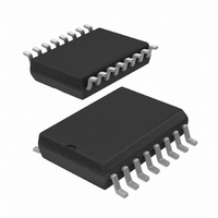
IC I/O EXPANDER I2C 8B 16SOIC
Manufacturer
NXP Semiconductors
Datasheet
1.PCF8574ATS3118.pdf
(24 pages)
Specifications of PCF8574AT/3,512
Package / Case
16-SOIC (0.300", 7.5mm Width)
Interface
I²C
Number Of I /o
8
Interrupt Output
Yes
Frequency - Clock
100KHz
Voltage - Supply
2.5 V ~ 6 V
Operating Temperature
-40°C ~ 85°C
Mounting Type
Surface Mount
Includes
POR
Logic Family
PCF
Number Of Lines (input / Output)
9
Operating Supply Voltage
2.5 V to 6 V
Power Dissipation
400 mW
Operating Temperature Range
- 40 C to + 85 C
Maximum Clock Frequency
100 KHz
Mounting Style
SMD/SMT
Number Of Output Lines
9
Output Current
25 mA
Output Voltage
2.4 V
Lead Free Status / RoHS Status
Lead free / RoHS Compliant
For Use With
568-3615 - DEMO BOARD I2C
Lead Free Status / Rohs Status
Lead free / RoHS Compliant
Other names
568-3987-5
935275581512
PCF8574ATD
PCF8574ATD
935275581512
PCF8574ATD
PCF8574ATD
Philips Semiconductors
7.2
The PCF8574 provides an open-drain output (INT) which
can be fed to a corresponding input of the microcontroller
(see Figs 13 and 14). This gives these chips a type of
master function which can initiate an action elsewhere in
the system.
An interrupt is generated by any rising or falling edge of the
port inputs in the input mode. After time t
valid.
Resetting and reactivating the interrupt circuit is achieved
when data on the port is changed to the original setting or
data is read from or written to the port which has generated
the interrupt.
Resetting occurs as follows:
2002 Nov 22
handbook, full pagewidth
handbook, full pagewidth
In the READ mode at the acknowledge bit after the rising
edge of the SCL signal
In the WRITE mode at the acknowledge bit after the
HIGH-to-LOW transition of the SCL signal
Remote 8-bit I/O expander for I
Interrupt output
DATA INTO
INT
P5
SDA
SCL
t iv
MICROCONTROLLER
start condition
S
Fig.14 Interrupt generated by a change of input to I/O P5.
INT
Fig.13 Application of multiple PCF8574s with interrupt.
0
1
slave address (PCF8574)
1
2
iv
0
3
the signal INT is
0
4
V DD
A2
5
2
C-bus
A1
6
PCF8574
A0
7
12
INT
(1)
R/W acknowledge
1
8
Each change of the I/Os after resetting will be detected
and, after the next rising clock edge, will be transmitted as
INT. Reading from or writing to another device does not
affect the interrupt circuit.
7.3
A quasi-bidirectional I/O can be used as an input or output
without the use of a control signal for data direction
(see Fig.15). At power-on the I/Os are HIGH. In this mode
only a current source to V
pull-up to V
outputs. These devices turn on when an output is written
HIGH, and are switched off by the negative edge of SCL.
The I/Os should be HIGH before being used as inputs.
Interrupts which occur during the acknowledge clock
pulse may be lost (or very short) due to the resetting of
the interrupt during this pulse.
A
from slave
t ir
PCF8574
Quasi-bidirectional I/Os
INT
(2)
DD
allows fast rising edges into heavily loaded
P5
1
data from port
DD
MBD976
PCF8574
is active. An additional strong
(16)
INT
Product specification
1
PCF8574
condition
MBD972
stop
P


