PCA9535BS,118 NXP Semiconductors, PCA9535BS,118 Datasheet - Page 9
PCA9535BS,118
Manufacturer Part Number
PCA9535BS,118
Description
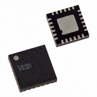
IC I/O EXPANDER I2C 16B 24HVQFN
Manufacturer
NXP Semiconductors
Datasheet
1.PCA9535BS118.pdf
(31 pages)
Specifications of PCA9535BS,118
Package / Case
24-VQFN Exposed Pad, 24-HVQFN, 24-SQFN, 24-DHVQFN
Interface
I²C, SMBus
Number Of I /o
16
Interrupt Output
Yes
Frequency - Clock
400kHz
Voltage - Supply
2.3 V ~ 5.5 V
Operating Temperature
-40°C ~ 85°C
Mounting Type
Surface Mount
Includes
POR
Logic Family
PCA9535
Number Of Lines (input / Output)
16.0 / 16.0
Operating Supply Voltage
2.3 V to 5.5 V
Power Dissipation
200 mW
Operating Temperature Range
- 40 C to + 85 C
Input Voltage
5 V
Logic Type
I2C, SMBus
Maximum Clock Frequency
400 KHz
Mounting Style
SMD/SMT
Number Of Input Lines
16.0
Number Of Output Lines
16.0
Output Current
50 mA
Output Voltage
5 V
Lead Free Status / RoHS Status
Lead free / RoHS Compliant
Lead Free Status / RoHS Status
Lead free / RoHS Compliant, Lead free / RoHS Compliant
Other names
568-3376-2
935273944118
PCA9535BS-T
935273944118
PCA9535BS-T
Available stocks
Company
Part Number
Manufacturer
Quantity
Price

Part Number:
PCA9535BS,118
Manufacturer:
NXP/恩智浦
Quantity:
20 000


NXP Semiconductors
PCA9535_PCA9535C_5
Product data sheet
6.5.1 Writing to the port registers
6.5 Bus transactions
Data is transmitted to the PCA9535/PCA9535C by sending the device address and
setting the least significant bit to a logic 0 (see
address”). The command byte is sent after the address and determines which register will
receive the data following the command byte.
The eight registers within the PCA9535/PCA9535C are configured to operate as four
register pairs. The four pairs are Input Ports, Output Ports, Polarity Inversion Ports, and
Configuration Ports. After sending data to one register, the next data byte will be sent to
the other register in the pair (see
sent to Output Port 1 (register 3), then the next byte will be stored in Output Port 0
(register 2). There is no limitation on the number of data bytes sent in one write
transmission. In this way, each 8-bit register may be updated independently of the other
registers.
Fig 7.
configuration
write polarity
shift register
shift register
shift register
write pulse
read pulse
data from
data from
data from
(1) PCA9535C I/Os are open-drain only. The portion of the PCA9535 schematic marked inside the
pulse
pulse
write
At power-on reset, all registers return to default values.
dotted line box is not in PCA9535C.
Simplified schematic of I/Os
configuration
register
D
CK
FF
Rev. 05 — 15 September 2008
Q
Q
16-bit I
output port
register
D
CK
2
Figure 8
FF
C-bus and SMBus, low power I/O port with interrupt
Q
and
PCA9535; PCA9535C
input port
register
polarity inversion
register
D
CK
D
CK
Figure
Figure 6 “PCA9535; PCA9535C device
FF
FF
Q
Q
9). For example, if the first byte is
(1)
Q1
Q2
© NXP B.V. 2008. All rights reserved.
output port
register data
V
I/O pin
V
input port
register data
to INT
polarity
inversion
register data
DD
SS
002aac218
9 of 31
Related parts for PCA9535BS,118
Image
Part Number
Description
Manufacturer
Datasheet
Request
R

Part Number:
Description:
NXP Semiconductors designed the LPC2420/2460 microcontroller around a 16-bit/32-bitARM7TDMI-S CPU core with real-time debug interfaces that include both JTAG andembedded trace
Manufacturer:
NXP Semiconductors
Datasheet:

Part Number:
Description:
NXP Semiconductors designed the LPC2458 microcontroller around a 16-bit/32-bitARM7TDMI-S CPU core with real-time debug interfaces that include both JTAG andembedded trace
Manufacturer:
NXP Semiconductors
Datasheet:
Part Number:
Description:
NXP Semiconductors designed the LPC2468 microcontroller around a 16-bit/32-bitARM7TDMI-S CPU core with real-time debug interfaces that include both JTAG andembedded trace
Manufacturer:
NXP Semiconductors
Datasheet:
Part Number:
Description:
NXP Semiconductors designed the LPC2470 microcontroller, powered by theARM7TDMI-S core, to be a highly integrated microcontroller for a wide range ofapplications that require advanced communications and high quality graphic displays
Manufacturer:
NXP Semiconductors
Datasheet:
Part Number:
Description:
NXP Semiconductors designed the LPC2478 microcontroller, powered by theARM7TDMI-S core, to be a highly integrated microcontroller for a wide range ofapplications that require advanced communications and high quality graphic displays
Manufacturer:
NXP Semiconductors
Datasheet:
Part Number:
Description:
The Philips Semiconductors XA (eXtended Architecture) family of 16-bit single-chip microcontrollers is powerful enough to easily handle the requirements of high performance embedded applications, yet inexpensive enough to compete in the market for hi
Manufacturer:
NXP Semiconductors
Datasheet:
Part Number:
Description:
The XA-S3 device is a member of Philips Semiconductors? XA(eXtended Architecture) family of high performance 16-bitsingle-chip microcontrollers
Manufacturer:
NXP Semiconductors
Datasheet:

Part Number:
Description:
The NXP BlueStreak LH75401/LH75411 family consists of two low-cost 16/32-bit System-on-Chip (SoC) devices
Manufacturer:
NXP Semiconductors
Datasheet:
Part Number:
Description:
The NXP LPC3130/3131 combine an 180 MHz ARM926EJ-S CPU core, high-speed USB2
Manufacturer:
NXP Semiconductors
Datasheet:
Part Number:
Description:
The NXP LPC3141 combine a 270 MHz ARM926EJ-S CPU core, High-speed USB 2
Manufacturer:
NXP Semiconductors
Part Number:
Description:
The NXP LPC3143 combine a 270 MHz ARM926EJ-S CPU core, High-speed USB 2
Manufacturer:
NXP Semiconductors

Part Number:
Description:
The NXP LPC3152 combines an 180 MHz ARM926EJ-S CPU core, High-speed USB 2
Manufacturer:
NXP Semiconductors
Part Number:
Description:
The NXP LPC3154 combines an 180 MHz ARM926EJ-S CPU core, High-speed USB 2
Manufacturer:
NXP Semiconductors

Part Number:
Description:
Standard level N-channel enhancement mode Field-Effect Transistor (FET) in a plastic package using NXP High-Performance Automotive (HPA) TrenchMOS technology
Manufacturer:
NXP Semiconductors
Datasheet: