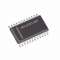
MAX261BEWG+ Maxim Integrated Products, MAX261BEWG+ Datasheet - Page 4

MAX261BEWG+
Manufacturer Part Number
MAX261BEWG+
Description
IC FILTER ACT MPU PROG 24-SOIC
Manufacturer
Maxim Integrated Products
Datasheet
1.MAX262BCNG.pdf
(26 pages)
Specifications of MAX261BEWG+
Filter Type
Universal Switched Capacitor
Frequency - Cutoff Or Center
57kHz
Number Of Filters
2
Max-order
2nd
Voltage - Supply
4.74 V ~ 12.6 V, ±2.37 V ~ 6.3 V
Mounting Type
Surface Mount
Package / Case
24-SOIC (7.5mm Width)
Lead Free Status / RoHS Status
Lead free / RoHS Compliant
INTERFACE SPECIFICATIONS (Note 9)
(V
Microprocessor Programmable
Universal Active Filters
ELECTRICAL CHARACTERISTICS (for V± = ±2.5V ±5%)
(V
MAX260/MAX261 and 139.80 for MAX262, Filter Mode 1, T
Note 9: Interface timing specifications are guaranteed by design and are not subject to test.
4
Note 1: f
Note 2: Q accuracy tested at Q = 8, 32, and 64. Q of 32 and 64 tested at 1/2 stated clock frequency.
Note 3: The offset voltage is specified for the entire filter. Offset is virtually independent of Q and f
Note 4: Output noise is measured with an RC output smoothing filter at 4
Note 5: TTL logic levels are: HIGH = 2.4V, LOW = 0.8V. CMOS logic levels are: HIGH = 5V, LOW = 0V. Power supply current is typi-
Note 6: On the MAX260 only, the HP output signal swing is typically 0.75V less than the LP or BP outputs.
Note 7: At ±2.5V supplies, the f
Note 8: f
f
Maximum Clock Frequency
f
(Notes 1, 8)
Q Accuracy (deviation from ideal
continuous filter)
(Notes 2, 8)
Output Signal Swing
Power Supply Current
Shutdown Current
0
CLK
WR Pulse Width
Address Setup
Address Hold
Data Setup
Data Hold
Logic Input High
Logic Input Low
Input Leakage Current
Input Capacitance
+
+
Center Frequency Range
= +5V, V
= +2.37V, V
_______________________________________________________________________________________
/f
0
Ratio Error
frequency for mode 3 is 175kHz for the MAX260 and 750kHz for the MAX261/MAX262.
cally 4mA higher with TTL logic and clock input levels.
as compared to ±5V; however, these parameters are only tested to the extent indicated by the MIN or MAX limits.
CLK
CLK
PARAMETER
PARAMETER
+
/f
/f
0
0
= -5V, T
-
accuracy is tested at 199.49 on the MAX260/MAX261, and at 139.8 on the MAX262.
and Q accuracy are a function of the accuracy of internal capacitor ratios. No increase in error is expected at ±2.5V
= -2.37V, CLK
A
= +25°C, unless otherwise noted.)
A
0
range and maximum clock frequency are typically 75% of values listed in Table 1.
= CLK
Q = 8
Q = 8
f
f
f
All Outputs (Note 6)
CMOS Level Logic Inputs (Note 5)
CMOS Level Logic Inputs (Note 5)
CLK
CLK
CLK
SYMBOL
t
B
t
t
V
C
/f
/f
/f
t
t
V
WR
I
AH
DH
AS
DS
IN
0
0
0
IH
IL
IN
= ±2.5V 250kHz for the MAX260 and 1MHz for the MAX261/MAX262, f
= 199.49
= 199.49
= 139.80
WR, D0, D1, A0–A3, CLK
T
WR, D0, D1, A0–A3, CLK
T
WR, D0, D1, A0–A3, CLK
CLK
T
WR, D0, D1, A0–A3, CLK
A
A
A
=T
=T
=T
A
MIN
MIN
MIN
CONDITIONS
A
= +25°C, unless otherwise noted.)
to T
to T
to T
MAX
MAX
MAX
CONDITIONS
MAX26XA
MAX26XB
MAX260A
MAX260B
MAX261A
MAX261B
MAX262A
MAX262B
✕
f
A
A
B
A
0
, CLK
, CLK
, CLK
to remove clock feedthrough.
B
B
B
MIN
MIN
250
100
CLK
2.4
25
10
0
/f
0
(Note 7)
(Note 7)
ratio setting. The test clock
TYP
±0.1
±0.1
0.35
TYP
150
±2
±2
±2
±2
±2
±2
±2
50
7
0
6
CLK
MAX
MAX
±10
±10
±10
±6
±6
±6
0.8
10
60
15
1
2
/f
0
= 199.49 for
UNITS
UNITS
mA
mA
%
%
µA
ns
ns
ns
ns
ns
pF
V
V
V


