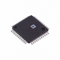
ADV7171KSU Analog Devices Inc, ADV7171KSU Datasheet - Page 28

ADV7171KSU
Manufacturer Part Number
ADV7171KSU
Description
IC DAC VIDEO ENC NTSC 44TQFP
Manufacturer
Analog Devices Inc
Type
Video Encoderr
Datasheet
1.ADV7171KSUZ.pdf
(64 pages)
Specifications of ADV7171KSU
Rohs Status
RoHS non-compliant
Applications
Set-Top Boxes, Video Players
Voltage - Supply, Analog
4.75 V ~ 5.25 V
Mounting Type
Surface Mount
Package / Case
44-TQFP, 44-VQFP
Adc/dac Resolution
10b
Screening Level
Industrial
Package Type
TQFP
Pin Count
44
Voltage - Supply, Digital
-
Lead Free Status / RoHS Status
Not Compliant
Available stocks
Company
Part Number
Manufacturer
Quantity
Price
Company:
Part Number:
ADV7171KSU
Manufacturer:
AD
Quantity:
319
Part Number:
ADV7171KSU
Manufacturer:
ADI/亚德诺
Quantity:
20 000
Company:
Part Number:
ADV7171KSUZ
Manufacturer:
LTC
Quantity:
20
Company:
Part Number:
ADV7171KSUZ
Manufacturer:
ADI
Quantity:
246
Company:
Part Number:
ADV7171KSUZ
Manufacturer:
Analog Devices Inc
Quantity:
10 000
Part Number:
ADV7171KSUZ
Manufacturer:
ADI/亚德诺
Quantity:
20 000
Company:
Part Number:
ADV7171KSUZ-REEL
Manufacturer:
SOURIAU
Quantity:
1 000
Company:
Part Number:
ADV7171KSUZ-REEL
Manufacturer:
Analog Devices Inc
Quantity:
10 000
ADV7170/ADV7171
REGISTER PROGRAMMING
This section describes each register, including subaddress
register, mode registers, subcarrier frequency registers,
subcarrier phase register, timing registers, closed captioning
extended data registers, closed captioning data registers, and
NTSC pedestal control registers, in terms of its configuration.
SUBADDRESS REGISTER (SR7 TO SR0)
The communications register is an 8-bit, write-only register.
After the part has been accessed over the bus and a read/write
operation is selected, the subaddress is set up. The subaddress
register determines to/from which register the operation takes
place.
Figure 37 shows the various operations under the control of the
subaddress register. Zero should always be written to SR7 to SR6.
REGISTER SELECT (SR5 TO SR0)
These bits are set up to point to the required starting address.
SEQUENCE
SEQUENCE
WRITE
READ
S SLAVE ADDR A(S)
S
S = START BIT
P = STOP BIT
SLAVE ADDR A(S)
LSB = 0
A(S) = ACKNOWLEDGE BY SLAVE
A(M) = ACKNOWLEDGE BY MASTER
SUBADDR
SUBADDR
Figure 36. Write and Read Sequences
A(S)
A(S) S SLAVE ADDR
Rev. C | Page 28 of 64
DATA
LSB = 1
A(S)
A (S) = NO-ACKNOWLEDGE BY SLAVE
A (M) = NO-ACKNOWLEDGE BY MASTER
A(S)
MODE REGISTER 0 MR0 (MR07 TO MR00)
(Address [SR4 to SR0] = 00H)
Figure 38 shows the various operations under the control of
Mode Register 0. This register can be read from as well as
written to.
MR0 BIT DESCRIPTION
Output Video Standard Selection (MR01 to MR00)
These bits are used to set up the encode mode. The ADV7170/
ADV7171 can be set up to output NTSC, PAL B/D/G/H/I, and
PAL M/N standard video.
Luminance Filter Control (MR02 to MR04)
These bits specify which luma filter is to be selected. The filter
selection is made independent of whether PAL or NTSC is
selected.
Chrominance Filter Control (MR05 to MR07)
These bits select the chrominance filter. A low-pass filter can be
selected with a choice of cutoff frequencies, 0.65 MHz,
1.0 MHz, 1.3 MHz, or 2 MHz, along with a choice of CIF
or QCIF filters.
DATA
DATA
A(M)
A(S) P
DATA
A(M) P


