ADV7171KSU Analog Devices Inc, ADV7171KSU Datasheet - Page 11
ADV7171KSU
Manufacturer Part Number
ADV7171KSU
Description
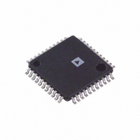
IC DAC VIDEO ENC NTSC 44TQFP
Manufacturer
Analog Devices Inc
Type
Video Encoderr
Datasheet
1.ADV7171KSUZ.pdf
(64 pages)
Specifications of ADV7171KSU
Rohs Status
RoHS non-compliant
Applications
Set-Top Boxes, Video Players
Voltage - Supply, Analog
4.75 V ~ 5.25 V
Mounting Type
Surface Mount
Package / Case
44-TQFP, 44-VQFP
Adc/dac Resolution
10b
Screening Level
Industrial
Package Type
TQFP
Pin Count
44
Voltage - Supply, Digital
-
Lead Free Status / RoHS Status
Not Compliant
Available stocks
Company
Part Number
Manufacturer
Quantity
Price

Company:
Part Number:
ADV7171KSU
Manufacturer:
AD
Quantity:
319
Part Number:
ADV7171KSU
Manufacturer:
ADI/亚德诺
Quantity:
20 000
Company:
Part Number:
ADV7171KSUZ
Manufacturer:
LTC
Quantity:
20
Company:
Part Number:
ADV7171KSUZ
Manufacturer:
ADI
Quantity:
246
Company:
Part Number:
ADV7171KSUZ
Manufacturer:
Analog Devices Inc
Quantity:
10 000
Part Number:
ADV7171KSUZ
Manufacturer:
ADI/亚德诺
Quantity:
20 000
Company:
Part Number:
ADV7171KSUZ-REEL
Manufacturer:
SOURIAU
Quantity:
1 000
Company:
Part Number:
ADV7171KSUZ-REEL
Manufacturer:
Analog Devices Inc
Quantity:
10 000


PIN CONFIGURATION AND FUNCTION DESCRIPTIONS
Table 9. Pin Function Descriptions
Pin No.
1, 11, 20, 28, 30
2 to 9, 12 to 14,
38 to 42
10, 19, 21, 29, 43
15
16
17
18
22
23
24
25
26
27
31
32
33
34
Mnemonic
V
P15 to P0
GND
HSYNC
FIELD/ VSYNC
BLANK
ALSB
RESET
SCLOCK
SDATA
COMP
DAC C
DAC D
DAC B
DAC A
V
R
SET
AA
REF
I
O
Input/
Output
P
I
G
I/O
I/O
I/O
I
I
I/O
O
O
O
O
I/O
I
GND
V
V
P10
P11
P12
AA
P5
P6
P7
P8
P9
AA
Description
Power Supply (3 V to 5 V).
8-Bit 4:2:2 Multiplexed YCrCb Pixel Port (P7 to P0) or 16-Bit YCrCb Pixel Port (P15 to P0).
P0 represents the LSB.
Ground Pin.
HSYNC (Mode 1 and Mode 2) Control Signal. This pin may be configured to output (master
mode) or accept (slave mode) sync signals.
Dual Function FIELD (Mode 1) and VSYNC (Mode 2) Control Signal. This pin may be
configured to output (master mode) or accept (slave mode) these control signals.
Video Blanking Control Signal. The pixel inputs are ignored when this is Logic Level 0. This
signal is optional.
TTL Address Input. This signal sets up the LSB of the MPU address.
The input resets the on-chip timing generator and sets the ADV7170/ADV7171 into default
mode. This is NTSC operation, Timing Slave Mode 0, 8-bit operation, 2 × composite and
S-Video out, and DAC B powered on and DAC D powered off.
MPU Port Serial Interface Clock Input.
MPU Port Serial Data Input/Output.
Compensation Pin. Connect a 0.1 μF capacitor from COMP to V
performance in low power mode, the value of the COMP capacitor can be lowered to as low
as 2.2 nF.
RED/S-Video C/V Analog Output.
GREEN/S-Video Y/Y Analog Output.
BLUE/Composite/U Analog Output.
PAL/NTSC Composite Video Output. Full-scale output is 180 IRE (1286 mV) for NTSC and
1300 mV for PAL.
Voltage Reference Input for DACs or Voltage Reference Output (1.235 V).
A 150 Ω resistor connected from this pin to GND is used to control full-scale amplitudes
of the video signals.
10
11
1
2
3
4
5
6
7
8
9
44 43 42 41 40 39 38 37 36 35 34
12 13 14 15 16 17 18 19 20 21 22
PIN 1
ADV7170/ADV7171
Figure 5. Pin Configuration
Rev. C | Page 11 of 64
(Not to Scale)
MQFP/TQFP
TOP VIEW
33
31
25
32
30
29
28
27
26
24
23
V
DAC A
DAC B
V
GND
V
DAC D
DAC C
COMP
SDATA
SCLOCK
REF
AA
AA
ADV7170/ADV7171
AA
. For optimum dynamic
Related parts for ADV7171KSU
Image
Part Number
Description
Manufacturer
Datasheet
Request
R

Part Number:
Description:
±1.7g Dual-Axis IMEMS Accelerometer Evaluation Board
Manufacturer:
Analog Devices Inc
Datasheet:

Part Number:
Description:
Inertial Sensor Evaluation System
Manufacturer:
Analog Devices Inc
Datasheet:
Part Number:
Description:
Manufacturer:
Analog Devices Inc
Datasheet:
Part Number:
Description:
Manufacturer:
Analog Devices Inc
Datasheet:
Part Number:
Description:
Manufacturer:
Analog Devices Inc
Datasheet:
Part Number:
Description:
Manufacturer:
Analog Devices Inc
Datasheet:
Part Number:
Description:
Manufacturer:
Analog Devices Inc
Datasheet:
Part Number:
Description:
Manufacturer:
Analog Devices Inc
Datasheet:
Part Number:
Description:
Manufacturer:
Analog Devices Inc
Datasheet:
Part Number:
Description:
Manufacturer:
Analog Devices Inc
Datasheet:
Part Number:
Description:
Manufacturer:
Analog Devices Inc
Datasheet:
Part Number:
Description:
Manufacturer:
Analog Devices Inc
Datasheet:
Part Number:
Description:
Manufacturer:
Analog Devices Inc
Datasheet: