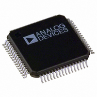
ADV7301AKST Analog Devices Inc, ADV7301AKST Datasheet - Page 46

ADV7301AKST
Manufacturer Part Number
ADV7301AKST
Description
IC DAC VIDEO HDTV 6-12BIT 64LQFP
Manufacturer
Analog Devices Inc
Type
Video Encoderr
Datasheet
1.ADV7301AKST.pdf
(68 pages)
Specifications of ADV7301AKST
Rohs Status
RoHS non-compliant
Applications
DVD, Set-Top Boxes
Voltage - Supply, Analog
2.37 V ~ 2.63 V
Voltage - Supply, Digital
2.37 V ~ 3.6 V
Mounting Type
Surface Mount
Package / Case
64-LQFP
Number Of Dac's
6
Adc/dac Resolution
12b
Screening Level
Commercial
Package Type
LQFP
Pin Count
64
Lead Free Status / RoHS Status
Compliant
Available stocks
Company
Part Number
Manufacturer
Quantity
Price
Company:
Part Number:
ADV7301AKST
Manufacturer:
AD
Quantity:
433
Company:
Part Number:
ADV7301AKST
Manufacturer:
ADI
Quantity:
300
Company:
Part Number:
ADV7301AKST
Manufacturer:
Analog Devices Inc
Quantity:
10 000
Part Number:
ADV7301AKSTZ
Manufacturer:
ADI/亚德诺
Quantity:
20 000
ADV7300A/ADV7301A
HD Sharpness Filter and Adaptive Filter Application Examples
HD Sharpness Filter Application
The HD sharpness filter can be used to enhance or attenuate
the Y video output signal.
The register settings in Tables XIX and XX are used to achieve
the results shown in Figure 64. Input data was generated by an
external signal source.
Address
00h
01h
02h
10h
11h
20h
20h
20h
20h
20h
20h
*See Figure 64.
The effect of the sharpness filter can also be seen when using the
internally generated crosshatch pattern.
Address
00h
01h
02h
10h
11h
20h
In toggling the Sharpness Filter Enable Bit [Address 11h,
Bit 8], it can be seen that the line contours of the crosshatch
pattern change their sharpness.
Table XX. Sharpness Filter on Internal Test Pattern
Table XIX. Sharpness Filter on Frequency Sweep
Figure 64. HD Sharpness Filter Control with Different Gain Settings for HD Sharpness Filter Gain Value
Register Setting
FCh
10h
20h
00h
81h
00h
08h
04h
40h
80h
22h
Register Setting
FCh
10h
20h
00h
85h
99h
Reference*
a
b
c
d
e
f
a
b
c
–46–
Adaptive Filter Control Application
Figure 65 shows a typical signal to be processed by the adaptive
filter control block.
The register settings in Table XXI are used to obtain the results
shown in Figure 66, i.e., to remove the ringing on the Y signal.
Input data was generated by an external signal source.
Figure 66. Output Signal After Adaptive Filter Control
Figure 65. Input Signal to Adaptive Filter Control
d
e
f
@: 446mV
@: 12.8ms
@: 446mV
@: 12.8ms
: 692mV
: 332ns
: 690mV
: 332ns
REV. A


