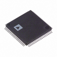
ADV7188BSTZ Analog Devices Inc, ADV7188BSTZ Datasheet - Page 30

ADV7188BSTZ
Manufacturer Part Number
ADV7188BSTZ
Description
IC DECODER VID MULTIFORM 80LQFP
Manufacturer
Analog Devices Inc
Type
Video Decoderr
Datasheet
1.ADV7188BSTZ.pdf
(112 pages)
Specifications of ADV7188BSTZ
Applications
Set-Top Boxes, Video Players, Recorders
Voltage - Supply, Analog
3.15 V ~ 3.45 V
Voltage - Supply, Digital
1.65 V ~ 2 V
Mounting Type
Surface Mount
Package / Case
80-LQFP
Resolution (bits)
12bit
Input Format
Analog
Output Format
Digital
Adc Sample Rate
54MSPS
No. Of Input Channels
12
Supply Voltage Range
3V To 3.6V
Lead Free Status / RoHS Status
Lead free / RoHS Compliant
Lead Free Status / RoHS Status
Lead free / RoHS Compliant, Lead free / RoHS Compliant
Available stocks
Company
Part Number
Manufacturer
Quantity
Price
Company:
Part Number:
ADV7188BSTZ
Manufacturer:
Analog Devices Inc
Quantity:
10 000
ADV7188
DEF_VAL_AUTO_EN, Default Value Automatic Enable,
Address 0x0C [1]
This bit enables the automatic use of the default values for Y, Cr,
and Cb when the ADV7188 cannot lock to the video signal.
0—Disables free-run mode. If the decoder is unlocked, it
outputs noise.
1 (default)—Enables free-run mode. A colored screen set by the
user-programmable Y, Cr, and Cb values is displayed when the
decoder loses lock.
CLAMP OPERATION
The input video is ac-coupled into the ADV7188 through a
0.1 μF capacitor. It is recommended that the range of the input
video signal is 0.5 V to 1.6 V (typically 1 V p-p). If the signal
exceeds this range, it cannot be processed correctly in the
decoder. Because the input signal is ac-coupled into the
decoder, its dc value needs to be restored. This process is
referred to as clamping the video. This section explains the
general process of clamping for the ADV7188 and shows the
different ways that a user can configure the device’s behavior.
The ADV7188 uses a combination of current sources and a
digital processing block for clamping, as shown in Figure 14.
There are three analog processing channels (like the one shown
in Figure 14) inside the IC. Although only one channel (and
only one ADC) is needed for a CVBS signal, two independent
channels are needed for S-video (Y/C) type signals, and three
independent channels are needed to allow component (YPrPb)
signals to be processed.
The clamping can be divided into two sections:
•
•
The ADCs can digitize an input signal only if it is within the 1.6 V
input voltage range. An input signal with a dc level that is too
large or too small is clipped at the top or bottom of the ADC range.
Clamping before the ADC (analog domain): current
sources
Clamping after the ADC (digital domain): digital
processing block
FINE-CURRENT SOURCES
ANALOG
VIDEO
INPUT
Figure 14. Clamping Overview
COARSE-CURRENT SOURCES
Rev. A | Page 30 of 112
ADC
The primary task of the analog clamping circuits is to ensure
that the video signal stays within the valid ADC input window
so that the analog-to-digital conversion can occur. Therefore,
precise clamping of the input signal within the analog domain
is unnecessary if the video signal fits within the ADC range.
After digitization, the digital fine-clamp block corrects for any
remaining variations in dc level. Because the dc level of an input
video signal refers directly to the brightness of the picture
transmitted, it is important to perform a fine clamp with high
accuracy; otherwise, brightness variations may occur. Further-
more, dynamic changes in the dc level usually lead to significant
artifacts and must therefore be prohibited.
The clamping scheme must be able to acquire a newly
connected video signal with a completely unknown dc level,
and it must maintain the dc level during normal operation.
To quickly acquire an unknown video signal, activate the large-
current clamps. It is assumed that the amplitude of the video
signal at this point is of a nominal value. Control of the coarse-
and fine-current clamp parameters is automatically performed
by the decoder.
Standard definition video signals may contain excessive noise.
In particular, CVBS signals transmitted by terrestrial broadcast
and then demodulated using a tuner usually show very large
levels of noise (>100 mV). A voltage clamp would be unsuitable
for this type of video signal. Instead, the ADV7188 uses a set of
four current sources that can cause coarse (>0.5 mA) and fine
(<0.1 mA) currents to flow into and away from the high
impedance node that carries the video signal (see Figure 14).
CCLEN, DCT [1:0], DCFE are the I
influence the behavior of the clamping block of the ADV7188.
CCLEN, Current Clamp Enable, Address 0x14 [4]
The current clamp enable bit allows the user to switch off the
current sources entirely in the analog front end. This may be
useful if the incoming analog video signal is clamped externally.
0—The current sources are switched off.
1 (default)—The current sources are enabled.
PREPROCESSOR
CLAMP CONTROL
(DPP)
DATA
WITH DIGITAL
FINE CLAMP
SDP
2
C signals that can be used to


