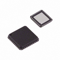
ADV7393BCPZ Analog Devices Inc, ADV7393BCPZ Datasheet - Page 19

ADV7393BCPZ
Manufacturer Part Number
ADV7393BCPZ
Description
IC DAC VIDEO HDTV 10BIT 40LFCSP
Manufacturer
Analog Devices Inc
Type
Video Encoderr
Datasheet
1.ADV7393BCPZ.pdf
(108 pages)
Specifications of ADV7393BCPZ
Design Resources
Reconstruction Video Filter Using ADA4430-1 Amplifier After ADV7393 Video Encoder (CN0101)
Applications
Set-Top Boxes, Video Players, Displays
Voltage - Supply, Analog
2.6 V ~ 3.46 V
Voltage - Supply, Digital
1.71 V ~ 1.89 V
Mounting Type
Surface Mount
Package / Case
40-LFCSP
Input Format
Digital
Output Format
Analog
Supply Voltage Range
1.71V To 1.89V
Operating Temperature Range
-40°C To +85°C
Tv / Video Case Style
LFCSP
No. Of Pins
40
Msl
MSL 1 - Unlimited
Lead Free Status / RoHS Status
Lead free / RoHS Compliant
For Use With
ADV7393-DBRDZ - BOARD EVAL FOR ADV7393EVAL-ADV7393EBZ - BOARD EVAL FOR ADV7393 ENCODER
Lead Free Status / RoHS Status
Lead free / RoHS Compliant, Lead free / RoHS Compliant
Available stocks
Company
Part Number
Manufacturer
Quantity
Price
Company:
Part Number:
ADV7393BCPZ
Manufacturer:
SIEMENS
Quantity:
101
Part Number:
ADV7393BCPZ
Manufacturer:
ADI/亚德诺
Quantity:
20 000
Company:
Part Number:
ADV7393BCPZ-3
Manufacturer:
ADI
Quantity:
302
Part Number:
ADV7393BCPZ-3
Manufacturer:
ADI/亚德诺
Quantity:
20 000
Company:
Part Number:
ADV7393BCPZ3
Manufacturer:
OSRAM
Quantity:
4 298
PIN CONFIGURATIONS AND FUNCTION DESCRIPTIONS
Table 15. Pin Function Descriptions
ADV7390/
ADV7391
9 to 7, 4 to 2,
31, 30
13
27
26
25
V
NOTES
1. THE EXPOSED PAD SHOULD BE CONNECTED
DGND
Figure 18. ADV7390/ADV7391 Pin Configuration
Figure 19. ADV7392/ADV7393 Pin Configuration
DD_IO
V
NOTES
1. THE EXPOSED PAD SHOULD BE CONNECTED
DGND
TO ANALOG GROUND (AGND).
V
P10
DD_IO
P4
P5
P6
P7
DD
P8
P9
TO ANALOG GROUND (AGND).
V
P2
P3
P4
DD
P5
P6
10
ADV7392/
ADV7393
18 to 15, 11 to
8, 5 to 2, 39 to
37, 34
19
33
32
31
1
2
3
4
5
6
7
8
9
1
2
3
4
5
6
7
8
Pin No.
PIN 1
INDICATOR
(Not to Scale)
(Not to Scale)
ADV7392/
ADV7390/
ADV7393
PIN 1
INDICATOR
ADV7391
TOP VIEW
TOP VIEW
ADV7390
WLCSP
F5, E5, E4, C5,
C4, B5, B4, A4
F4
A2
B2
B3
24 R
23 COMP
22 DAC 1
21 DAC 2
20 DAC 3
19 V
18 AGND
17 PV
30 R
29 COMP
28 DAC 1
27 DAC 2
26 DAC 3
25 V
24 AGND
23 PV
22 EXT_LF
21 PGND
AA
SET
AA
SET
DD
DD
Mnemonic
P7 to P0
P15 to P0
CLKIN
HSYNC
VSYNC
SFL
Rev. B | Page 19 of 108
Input/
Output
I
I
I
I/O
I/O
I/O
ADV7390/ADV7391/ADV7392/ADV7393
Description
8-Bit Pixel Port (P7 to P0). P0 is the LSB. See Table 35 for
input modes (ADV7390/ADV7391).
16-Bit Pixel Port (P15 to P0). P0 is the LSB. See Table 36 for
input modes (ADV7392/ADV7393).
Pixel Clock Input for HD (74.25 MHz), ED
or SD (27 MHz).
Horizontal Synchronization Signal. This pin can also be
configured to output an SD, ED, or HD horizontal
synchronization signal. See the External Horizontal and
Vertical Synchronization Control section.
Vertical Synchronization Signal. This pin can also be
configured to output an SD, ED, or HD vertical
synchronization signal. See the External Horizontal and
Vertical Synchronization Control section.
Subcarrier Frequency Lock (SFL) Input. The SFL input is
used to drive the color subcarrier DDS system, timing
reset, or subcarrier reset.
A
B
C
D
E
F
Figure 20. ADV7390BCBZ-A Pin Configuration
BALL A1 CORNER
AGND
PGND
DAC1
PV
R
V
SET
1
AA
DD
COMP
GND_IO
EXT_LF
HSYNC
VSYNC
SDA
2
(BALL SIDE DOWN)
Not to Scale
TOP VIEW
DGND
RESET
ALSB
SCL
V
SFL
3
DD
CLKIN
V
P0
P1
P3
P5
4
DD
1
DGND
V
(27 MHz or 54 MHz),
DD_IO
P2
P4
P6
P7
5


